Semiconductor Gas Sensor And Method For Producing The Same

a technology of semiconductor devices and gas sensors, applied in semiconductor devices, material analysis, instruments, etc., can solve the problems of gas sensor not responding to hydrogen, gas sensor lack of reliability, basic technique of gate electrodes, etc., and achieve the effect of increasing the response speed

Active Publication Date: 2013-11-28
HITACHI LTD
View PDF3 Cites 19 Cited by
  • Summary
  • Abstract
  • Description
  • Claims
  • Application Information

AI Technical Summary

Benefits of technology

[0024]Further, a semiconductor gas sensor which can be operated in a high-temperature environment (e.g., from 300° C. to 900° C.) without deteriorating the rising response speed and a method for producing the same can be provided.

Problems solved by technology

However, such a gas sensor has a problem of lack of reliability (e.g., Introduction of T. Usagawa et al., Journal of Applied Physics, Vol. 108, 074909 (2010) (NPL 2)).
However, the insertion of such an adhesive film caused a problem that the gas sensor does not respond to hydrogen.
However, a sensor signal drifts or an unidentified signal of as much as about 0.6 V is detected even at a low concentration (52.2 ppm), and a basic technique for a gate electrode, a passivation film, a source-drain electrode, a heater, etc. capable of operating stably at a high temperature for a long period of time has not been established yet.
In particular, other than the problem of reliability attributed to crystallinity, the fact that a gate electrode having high reliability has not been found yet is the biggest obstacle to putting it into practical use.
For example, the biggest obstacle to obtaining reliability of a Pt gate structure is as follows.
Due to this, a problem arises in sensor signal drift at a high temperature and reproducibility.

Method used


Image

  • Semiconductor Gas Sensor And Method For Producing The Same
  • Semiconductor Gas Sensor And Method For Producing The Same
  • Semiconductor Gas Sensor And Method For Producing The Same

Examples


first embodiment

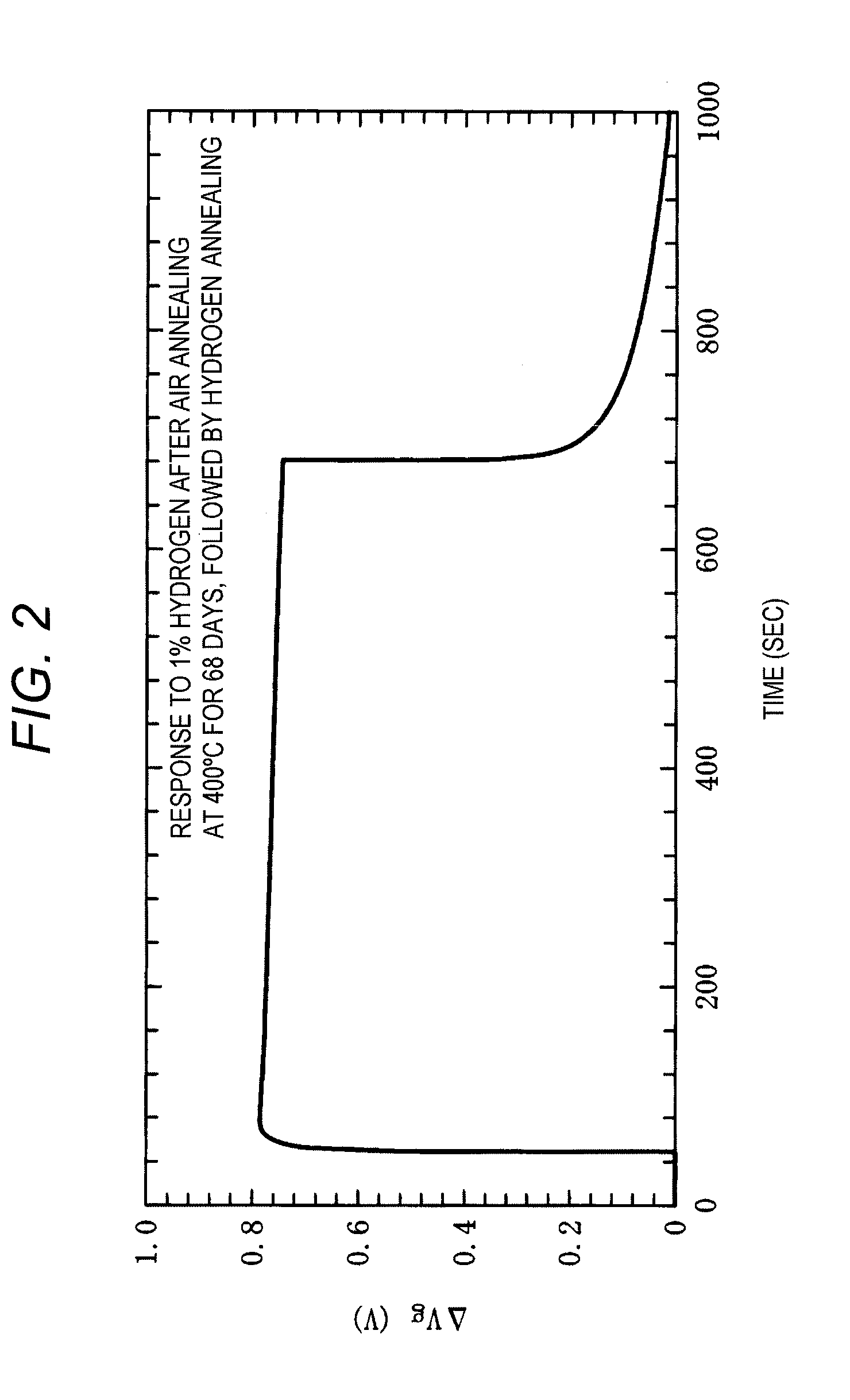
[0082]The present inventors performed annealing (a heat treatment) of a Si-MISFET having a Pt—Ti—O gate structure in an air atmosphere at 400° C. for 68 days. The thickness of a Pt film is 15 nm, the thickness of a Ti film is 5 nm, and the thickness of a SiO2 film is 18 nm. The gate length (Lg) is 10 μm, and the gate width (Wg) is 150 μm. It was found that by performing this treatment, the structure is changed such that a TiOx nanocrystal (a TiOx microcrystal) in a modified Ti film grows large, and an oxygen-doped amorphous Ti region is significantly reduced (hereinafter, a crystalline film composed of a TiOx nanocrystal (a TiOx microcrystal) is referred to as a modified TiOx film). This phenomenon occurs in an extremely thin film having a thickness of about 5 nm, and in a common bulk Ti film, a TiOx nanocrystal does not grow large. The phenomenon in which a TiOx nanocrystal in a modified Ti film grows large even at a relatively low temperature as compared with the melting point (17...

second embodiment

[0122]The modified Pt—Ti—O gate structure is stabilized by annealing at 400° C. over a long period of time of 68 days, and therefore, by applying the modified Pt—Ti—O gate structure to a SiC-MISFET gate electrode, stable operation can be achieved at a temperature of about 400° C. for a long period of time. A point that the modified Pt—Ti—O / SiO2 / SiC substrate structure adopting this gate structure is very stable is different from the Pt (100 nm) / SiO2 / SiC substrate structure (“Pt 100 nm” is described on the third line from the bottom of the left column in page 201 of the above-described NPL 4) in the related art.

[0123]In a production process of forming a SiC-MISFET-type gas sensor, after forming a gate insulating film (e.g., a SiO2 film), hydrogen annealing is performed at 800° C. to 1000° C. for about 30 minutes, whereby hydrogen termination is performed in the vicinity of a SiO2 / SiC boundary surface. By doing this, a phenomenon in which terminating hydrogen starts to be desorbed (a ...

third embodiment

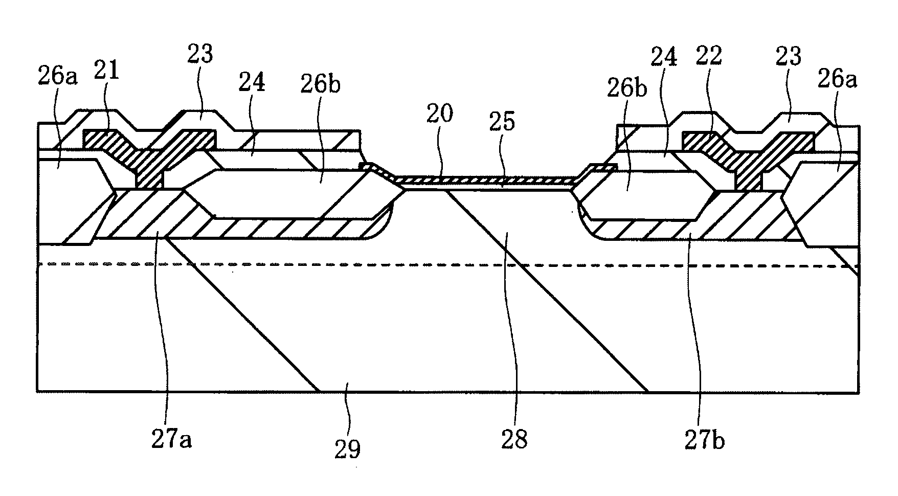
[0151]In the above-described second embodiment, as the gate electrode of the SiC-MISFET, a modified Pt—Ti—O gate structure is applied, and therefore, the operation temperature capable of ensuring reliability is up to 630° C. In order to ensure a temperature higher than 630° C., for example, a temperature up to 930° C. as the operation temperature capable of ensuring reliability, a modified Ir—Ti—O gate structure is needed. A gate portion and a heater wiring portion are different from those in the above-described second embodiment, and therefore, different points from the above-described second embodiment will be mainly explained.

[0152]The basic structure of the SiC-MISFET-type gas sensor having a modified Ir—Ti—O gate structure according to the third embodiment will be described with reference to FIGS. 10 to 11B.

[0153]FIG. 10 is an enlarged schematic cross-sectional view of a part of a gate structure of the SiC-MISFET having a modified Ir—Ti—O gate structure according to the third e...


PUM


Abstract

A technique capable of realizing a semiconductor gas sensor having a high rising response speed is provided. A gate insulating film (e.g., a SiO2 film) is formed on a Si layer, and a modified TiOx (a TiOx nanocrystal) film is formed on the gate insulating film. Further, on the modified TiOx film, a Pt film is formed. This Pt film is composed of a plurality of Pt crystal grains, and in a crystal grain boundary gap existing among the plurality of Pt crystal grains, Ti and oxygen (O) are present, and particularly, a TiOx nanocrystal is formed on a surface in the vicinity of a grain boundary triple point as the center.

Description

[0001]This application claims the priority of Japanese Patent Application No. JP 2012-116874, filed May 22, 2012, the disclosure of which is expressly incorporated by reference herein in its entirety.BACKGROUND OF THE INVENTION[0002]1. Field of the Invention[0003]The present invention relates to a gas sensor using a semiconductor material (a semiconductor gas sensor) and a technique for producing the same, and particularly relates to a semiconductor gas sensor, which is suitable for detecting hydrogen gas, has high reliability and high sensitivity, and can be applied also to an operation in a high temperature environment, and an effective technique to be applied to the production thereof.[0004]2. Background Art[0005]As a gas sensor to be used for detecting hydrogen gas, there are provided a Si-MOSFET (a metal-oxide-semiconductor field-effect transistor) type gas sensor having a Pd (palladium) gate structure (e.g., I. Lundstrom et al., Applied Physics Letters, Vol. 26, No. 2, 15 Janu...

Claims


Application Information

Patent Timeline
Patent Type & Authority Applications(United States)
IPC IPC(8): H01L29/78H01L29/66
CPCH01L29/78H01L29/66477G01N27/4141
Inventor USAGAWA, TOSHIYUKI
Owner HITACHI LTD
Why Eureka
Try Eureka