Semiconductor Device Manufacturing Method

Active Publication Date: 2013-11-28
INST OF MICROELECTRONICS CHINESE ACAD OF SCI
View PDF6 Cites 33 Cited by
  • Summary
  • Abstract
  • Description
  • Claims
  • Application Information

AI Technical Summary

Benefits of technology

[0026]According to one aspect of the present invention, the diffusion barrier layer is used for preventing diffusion of boron ions implanted into the source/drain region for a PMOS.
[0027]The advantages of the present invention are to provide a manufacturing method for a semiconductor device having epitaxial source/drain regions, in which a diffusion barrier layer of the source/drain regions made of epitaxial silicon-carbon or germanium silicon-carbon are added on the basis of epitaxially growing germanium-silicon of the source/drain regions in the prior art process, and the introduction of the diffusion barrier layer of

Problems solved by technology

After semiconductor integrated circuit technology enters into technical node of 90 nm feature size, maintaining or improving transistor performance is becoming more and more challenging.
In addition, if boron diffuses from source/drain extension regions into a gate insulating layer, the electrical properties of the gate insulating layer will become unstable.
All the above three aspects will degrade the electrical performance of the devices.
In PMOS, boron diffusing into the channel may result in a reduction of the threshold voltage in devices with small size.
If the HALO implantation is performed before the epitaxial growth, the high dosage implantation may destroy the crystal structure at the surfaces of the source/drain trenches, thus influencing the subsequent epitaxial growth of ge

Method used


Image

  • Semiconductor Device Manufacturing Method
  • Semiconductor Device Manufacturing Method
  • Semiconductor Device Manufacturing Method

Examples


Example

[0030]The present invention will be described below by the specific embodiments shown in the figures. It shall be understood that these descriptions are exemplary and are not intended to limit the scope of the present invention. In addition, descriptions about the known structures and techniques are omitted so as not to unnecessarily confusing the concepts of the present invention.

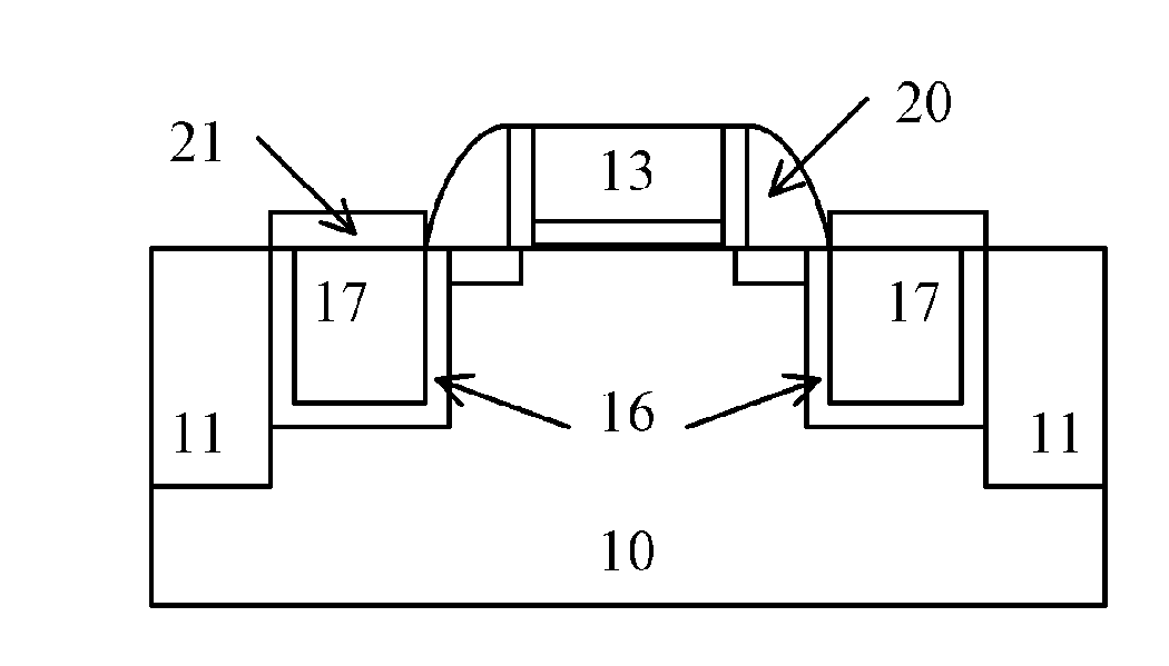
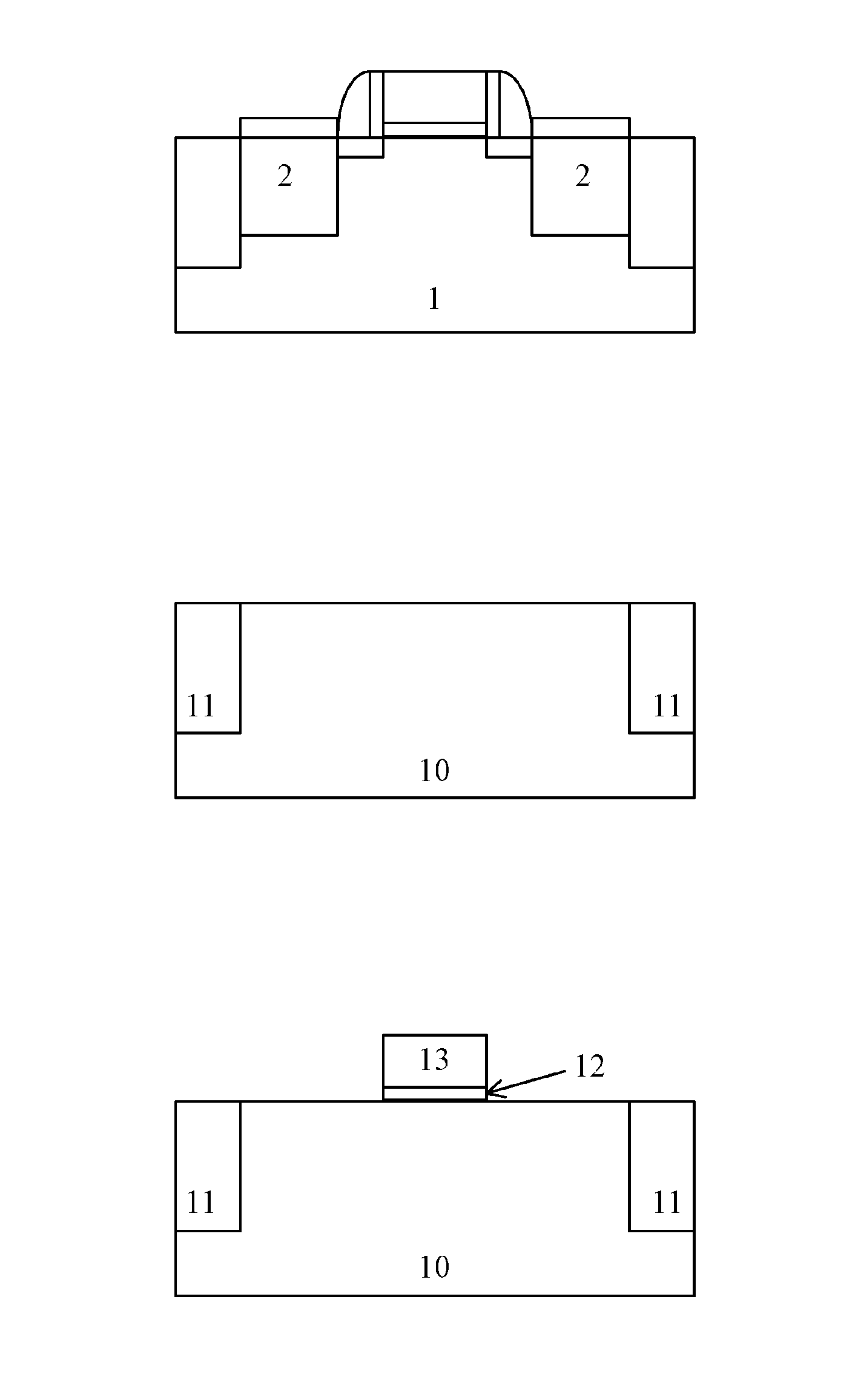
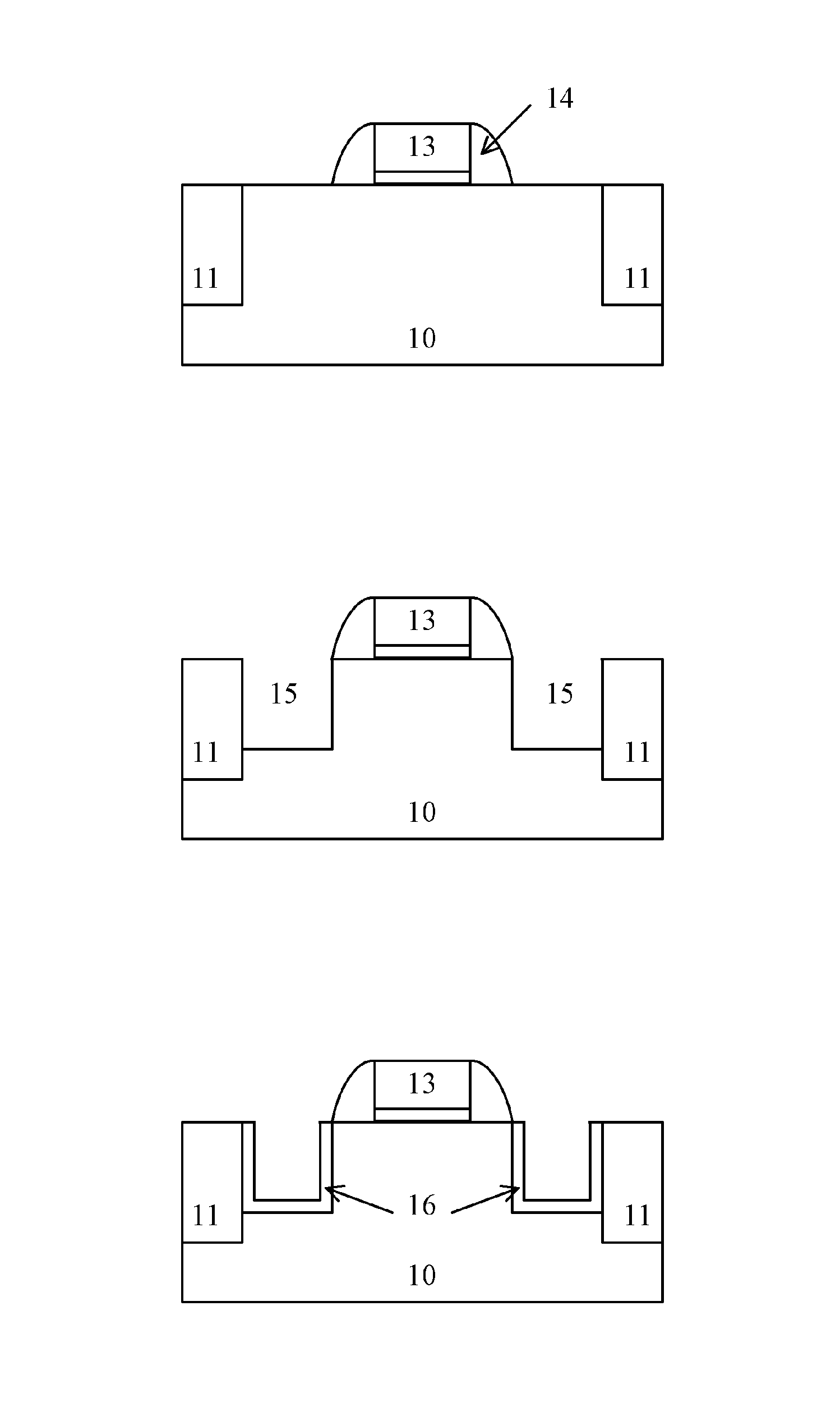
[0031]The present invention provides a semiconductor device manufacturing method, in particular to a manufacturing method for a transistor having epitaxial source / drain regions, and the manufacturing process thereof is as shown in FIGS. 2-11.

[0032]Referring to FIG. 2 first, STIs (Shallow Trench isolation) 11 are formed in a semiconductor substrate 10 and well region implantation is performed. The semiconductor substrate 10 is monocrystalline silicon in this embodiment. Alternatively, an SOI substrate or other suitable semiconductor substrates can also be used. STIs 11 are formed in the semiconductor substr...


PUM


Abstract

The present invention provides a manufacturing method for a semiconductor device having epitaxial source/drain regions, in which a diffusion barrier layer of the source/drain regions made of epitaxial silicon-carbon or germanium silicon-carbon are added on the basis of epitaxially growing germanium-silicon of the source/drain regions in the prior art process, and the introduction of the diffusion barrier layer of the source/drain regions prevents diffusion of the dopant in the source/drain regions, thus mitigating the SCE and DIBL effect. The use of the diffusion barrier layer for the source/drain regions can also reduce the dosage of HALO implantation in the subsequent step, thus if HALO is performed before epitaxial growth of the source/drain regions, impact on the surfaces of the source/drain regions can be alleviated; if HALO is performed after epitaxial growth of the source/drain regions, the stress release effect of the epitaxial layer of the source drain/regions caused by the implantation can be reduced as much as possible.

Description

CROSS REFERENCE[0001]This application is a National Stage Application of, and claims priority to, PCT Application No. PCT / CN2012 / 000803, filed on Jun. 12, 2012, entitled “Semiconductor Device Manufacturing Method”, which claims priority to Chinese Application No. 201210168214.0, filed on May 25, 2012. Both the PCT application and the Chinese application are incorporated herein by reference in their entireties.FIELD OF THE INVENTION[0002]The present invention relates to a semiconductor device manufacturing method, in particular to a manufacturing method for a transistor having epitaxial source / drain regions.BACKGROUND OF THE INVENTION[0003]After semiconductor integrated circuit technology enters into technical node of 90 nm feature size, maintaining or improving transistor performance is becoming more and more challenging. In the current mainstream technology, the performance of PMOS is improved by epitaxially growing germanium-silicon in trenches of source / drain regions to provide a...

Claims


Application Information

Patent Timeline
IPC IPC(8): H01L21/336
CPCH01L29/165H01L29/6653H01L29/6659H01L29/66636H01L29/7833H01L29/7848
Inventor QIN, CHANGLIANGYIN, HUAXIANG
Owner INST OF MICROELECTRONICS CHINESE ACAD OF SCI
Why Eureka
Try Eureka