Inductor device and fabrication method

a technology of inductors and fabrication methods, applied in semiconductor devices, semiconductor/solid-state device details, inductances, etc., can solve problems such as low quality factor, affecting the performance of planar inductors, and process uniformity and stability

Active Publication Date: 2013-12-12
SEMICON MFG INT (SHANGHAI) CORP
View PDF11 Cites 14 Cited by
  • Summary
  • Abstract
  • Description
  • Claims
  • Application Information

AI Technical Summary

Benefits of technology

[0007]According to various embodiments, there is provided an inductor device. The inductor device can include a first planar spiral wiring disposed over a semiconductor substrate; a second planar spiral wiring disposed over the first planar spiral wiring; and a third planar spiral wiring disposed over the second planar spiral wiring. Each of the first, the second, and the third planar spiral wirings can include an outer spiral metal wiring and an inner spiral metal wiring. The inner spiral metal wiring can include at least two isolated sub-metal-lines each connecting to the outer spiral metal wiring. One sub-metal-line of the at least two isolated sub-metal-lines in each of the first, the second, and the third planar spiral wirings can be connected to one another, and the outer spiral metal wiring in the first planar spiral wiring can be connected to the outer spiral metal wiring in the third planar spiral wiring such that the first and the third planar spiral wirings are configured in parallel and the second planar spiral wiring is configured in series with the first and the third planar spiral wirings configured in parallel.
[0023]To improve the quality factor and device performance, the width of the metal wire may be increased, so that the current density in the metal wire increases, thereby reducing resistance of the metal wire. However, when the width increases, the overlapping area between the metal wire and adjacent components may also be increased. Parasitic capacitance may be increased as well. As disclosed herein, certain approaches may be used to reduce width of the metal wire and to reduce the effective area of the inductor device. In addition, the resistance and parasitic capacitance can be reduced by controlling various configurations of the planar spiral wiring(s) and their sub-metal-lines. For example, the planar spiral wiring(s) can be configured in parallel, in series, and / or in combination of the parallel and series configurations.

Problems solved by technology

With downsizing of IC devices, there are challenges on process uniformity and stability.
However, such planar inductor often has a low quality factor, which may affect performance of the planar inductor.

Method used


Image

  • Inductor device and fabrication method
  • Inductor device and fabrication method
  • Inductor device and fabrication method

Examples


Embodiment Construction

[0020]Reference will now be made in detail to exemplary embodiments of the disclosure, which are illustrated in the accompanying drawings. Wherever possible, the same reference numbers will be used throughout the drawings to refer to the same or like parts.

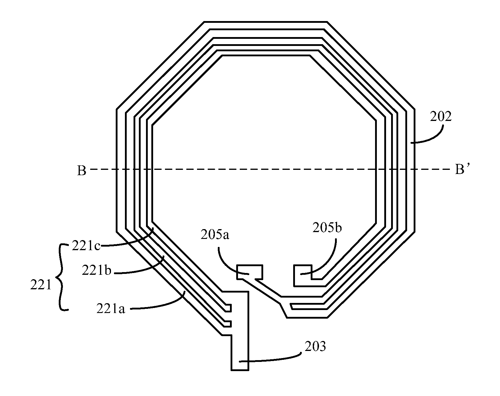
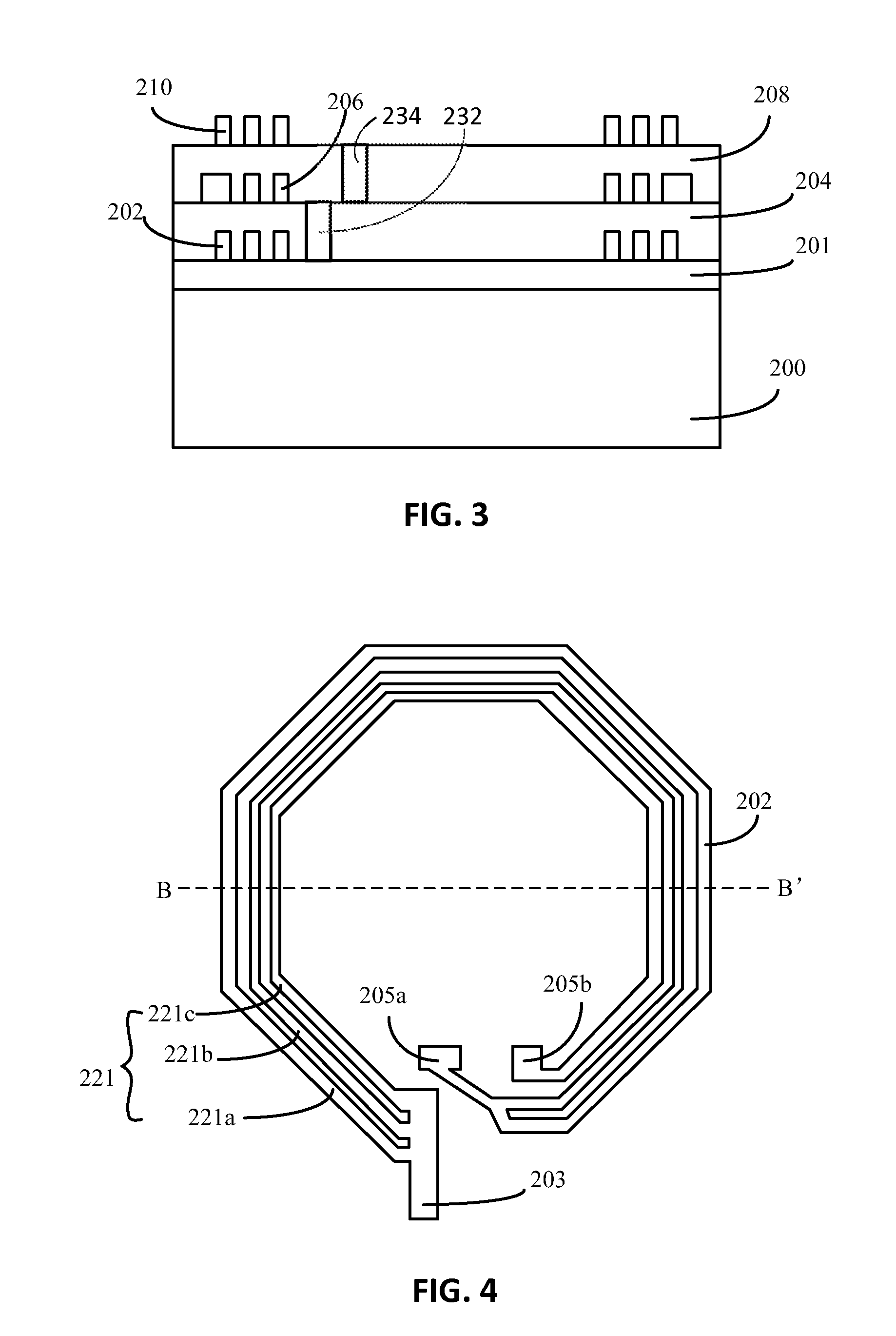
[0021]Various embodiments provide inductor devices and fabrication methods. An exemplary inductor device can include a plurality of planar spiral wirings (e.g., formed by conductive coils) isolated by a dielectric layer. The planar spiral wirings can be connected by conductive pads formed over the dielectric layer and by conductive plugs formed in the dielectric layer. In one embodiment, a third planar spiral wiring can be formed over a second planar spiral wirings that is formed over a first planar spiral wiring. The third planar spiral wiring can be configured in parallel with the first third planar spiral wiring. The second planar spiral wiring can be configured in series with the first and third planar spiral wirings configure...


PUM


Abstract

Various embodiments provide inductor devices and fabrication methods. An exemplary inductor device can include a plurality of planar spiral wirings isolated by a dielectric layer. The planar spiral wirings can be connected by conductive pads formed over the dielectric layer and by conductive plugs formed in the dielectric layer. In one embodiment, a third planar spiral wiring can be formed over a second planar spiral wirings that is formed over a first planar spiral wiring. The third planar spiral wiring can be configured in parallel with the first third planar spiral wiring. The second planar spiral wiring can be configured in series with the first and third planar spiral wirings configured in parallel.

Description

CROSS-REFERENCES TO RELATED APPLICATIONS[0001]This application claims priority to Chinese Patent Application No. CN201210184958.1, filed on Jun. 6, 2012, the entire contents of which are incorporated herein by reference.FIELD OF THE DISCLOSURE[0002]The present disclosure relates to the field of semiconductor technology and, more particularly, relates to inductor devices and methods of fabricating high-performance inductor devices.BACKGROUND[0003]In integrated circuits (ICs), such as complementary metal-oxide-semiconductor (CMOS) radio frequency integrated circuit (RFIC), inductors are important circuitry component, whose performance parameters may directly affect the performance of the ICs. Current inductors often include planar spiral inductors made of metal wires disposed on surface of a substrate or a dielectric layer of an IC device. Planar spiral inductors typically have low noise and low power consumption and are easy for device integration with low cost. With downsizing of IC...

Claims


Application Information

Patent Timeline
Patent Type & Authority Applications(United States)
IPC IPC(8): H01L49/02
CPCH01L28/10H01L21/76897H01L23/5227H01L2924/0002
Inventor CHENG, JENHAOWANG, XININGLIU, LING
Owner SEMICON MFG INT (SHANGHAI) CORP
Why Eureka
Try Eureka