MEMS inertial sensor and forming method therefor

a technology of inertial sensor and inertial sensor, which is applied in the field of semiconductors, can solve the problems of reducing production yield, affecting device reproducibility and film thickness, and limiting the size and sensitivity of inertial sensor, so as to improve the reproducibility and yield of fabricating the inertial sensor increase the mass of the element, and improve the sensitivity and reliability of the inertial sensor

Active Publication Date: 2013-12-26
MEMSEN ELECTRONICS
View PDF9 Cites 5 Cited by
  • Summary
  • Abstract
  • Description
  • Claims
  • Application Information

AI Technical Summary

Benefits of technology

[0009]An object of the invention is to provide a MEMS inertial sensor and a method for forming the same, in order to overcome the shortcomings of MEMS inertial sensor in the prior art such as poor reliability and reproducibility, and low yield.
[0031]As compared with the prior art, the technical solutions of the invention have the following advantages. Since the sensitive element of the sensor is formed of monocrystalline semiconductor material (the first substrate), thicker movable sensitive element, i.e., the movable electrode, of the inertial sensor may be formed, thereby increasing the mass of the element, and improving the sensitivity and reliability of the MEMS inertial sensor. Moreover, since the sensitive element of the sensor is formed of monocrystalline semiconductor material (the first substrate), the reproducibility and the yield of fabricating the MEMS inertial sensor can be improved.
[0032]Moreover, in the embodiment of the invention, one or more conductive layers are formed on the first substrate, and the one or more conductive layers may be used to fabricate the electrical shielding layer of the MEMS inertial sensor, the interconnecting layer of the MEMS inertial sensor, the fixed electrode of the MEMS inertial sensor, the supporting post of the fixed electrode of the MEMS inertial sensor, the supporting post of the movable sensitive element of the MEMS inertial sensor, or any combination thereof. Thus, the manufacturing process is simpler, the flexibility for manufacturing the MEMS inertial sensor is enhanced, the layout becomes easier, and the flexibility for integrating with other devices is improved. The electrical shielding layer is electrically connected with the shielding interconnecting line of the interconnecting layer, and therefore the MEMS inertial sensor is shielded from external interference.
[0033]Moreover, in the embodiments of the invention, the MEMS inertial sensor includes an anti-stiction structure which is fabricated by using the first substrate or the one or more conductive layers, and thus the process for forming the anti-stiction structure is simple.

Problems solved by technology

The polycrystalline silicon method has the advantage of simple process, but the material has relatively high stress, which affects device reproducibility and increase in film thickness, and therefore limits the size and sensitivity of the inertial sensor.
Moreover, due to the poor reproducibility, production yield is reduced, and cost is increased.
But due to the inherent disadvantage of etching technology, i.e., non-uniformity, the performance of the formed sensor such as the reliability may be affected.
Moreover, in the aforementioned US patent, the Z-axis sensor detects the Z-axis acceleration by detecting the change in overlapping area between the capacitor electrodes due to the displacement in the vertical direction, thereby limiting the design of the vertical-direction (Z-axis) sensor.

Method used


Image

  • MEMS inertial sensor and forming method therefor
  • MEMS inertial sensor and forming method therefor
  • MEMS inertial sensor and forming method therefor

Examples


Embodiment Construction

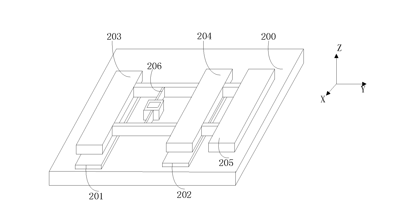
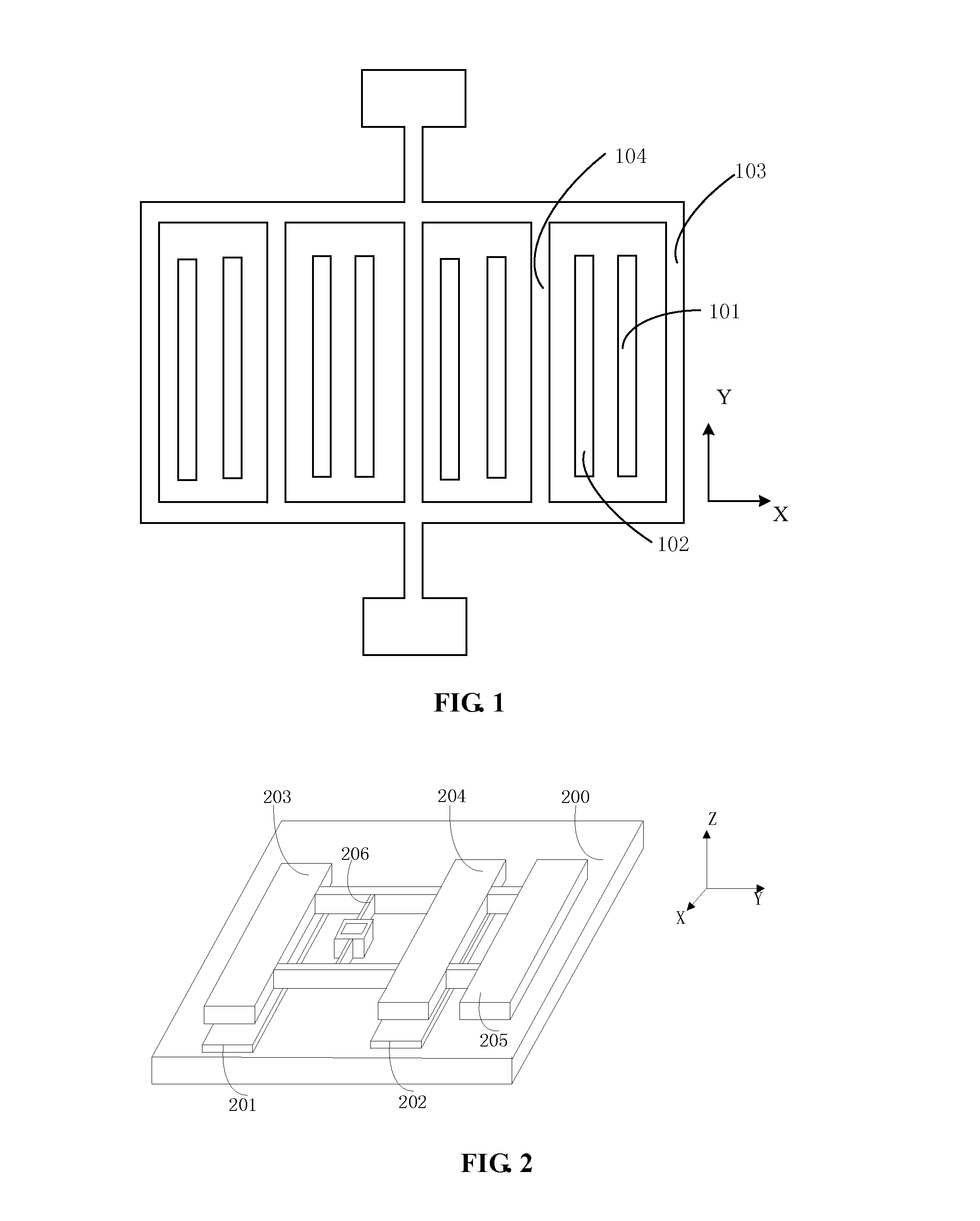
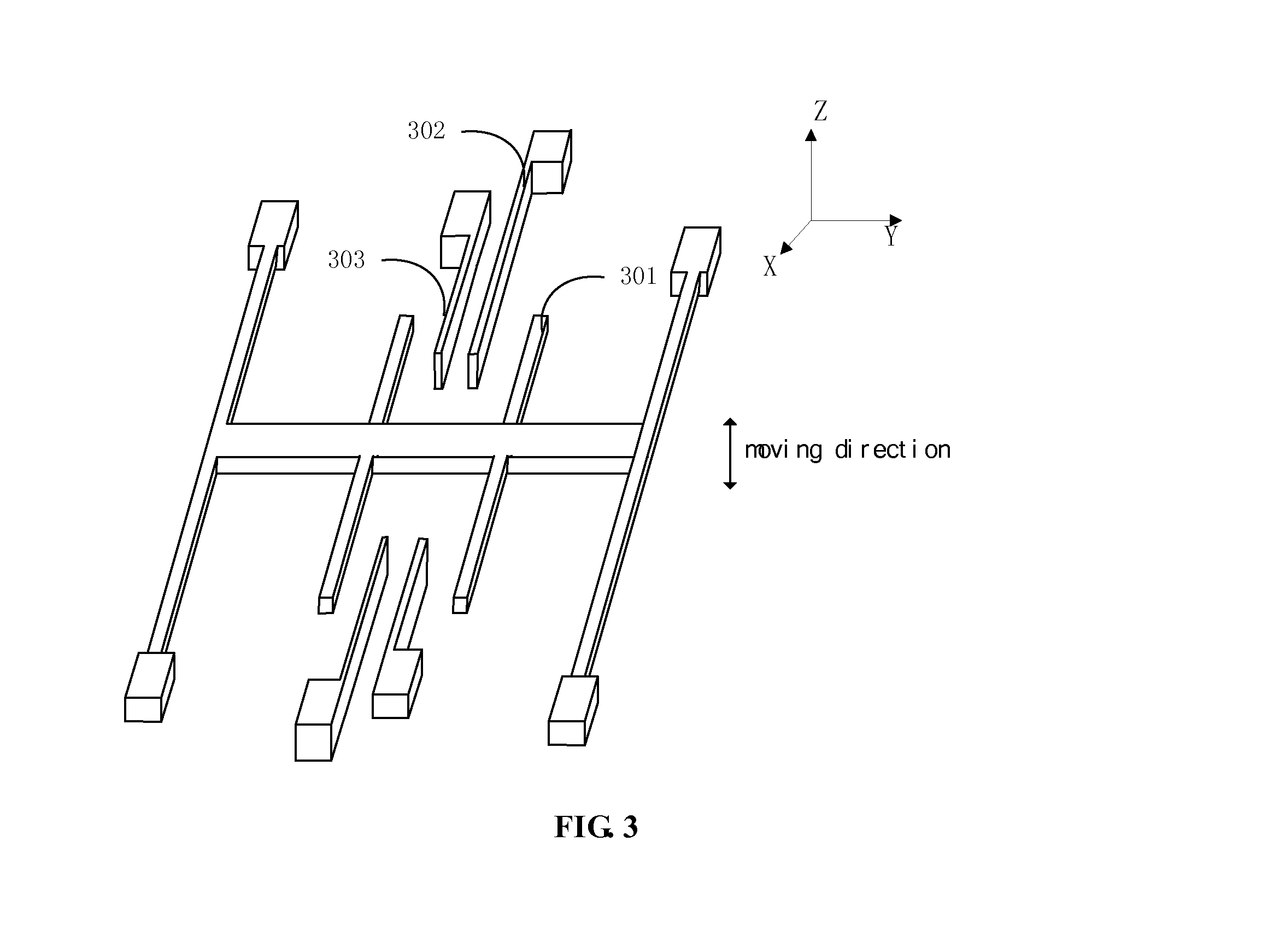
[0044]In the embodiments of the invention, since the sensitive element of the sensor is formed of monocrystalline semiconductor material (the first substrate), thicker movable sensitive element, i.e., the movable electrode, of the inertial sensor may be formed, therefore improving the sensitivity and reliability of the MEMS inertial sensor. Moreover, since the sensitive element of the sensor is formed of monocrystalline semiconductor material (the first substrate), the reproducibility and the yield of fabricating the MEMS inertial sensor can be improved.

[0045]Moreover, in the embodiments of the invention, one or more conductive layers are formed on the first substrate, and the one or more conductive layers may be used to fabricate the electrical shielding layer of the MEMS inertial sensor, the interconnecting layer of the MEMS inertial sensor, the fixed electrode of the MEMS inertial sensor, the supporting post of the fixed electrode of the MEMS inertial sensor, the supporting post ...


PUM

PropertyMeasurementUnit
conductiveaaaaaaaaaa
electricalaaaaaaaaaa
velocityaaaaaaaaaa

Abstract

A MEMS inertial sensor, may include a movable sensitive element; and second substrate and a third substrate. The movable sensitive element may be formed by using a first substrate which may be formed of a monocrystalline semiconductor material. The first substrate may include a first surface and a second surface which are opposite to each other. One or more conductive layers may be formed on the first surface of the first substrate The second substrate may be coupled to a surface of the one or more conductive layer on the first substrate. The third substrate may be coupled to the second surface of the first substrate. The third substrate and the second substrate are respectively arranged on two opposite sides of the movable sensitive element.

Description

CROSS REFERENCE TO RELATED APPLICATIONS[0001]This is the US national stage of application No. PCT / CN2012 / 071495 filed on Feb. 23, 2012. Priority under 35 U.S.C. §119(a) and 35 U.S.C. §365(b) is claimed from Chinese Application No. 201110061571.2, filed on Mar. 15, 2011, the disclosure of which is incorporated herein by reference in its entirety.FIELD OF THE INVENTION[0002]The present invention relates to the technical field of semiconductor, and in particular to a MEMS inertial senor and a method for forming the same.BACKGROUND OF THE INVENTION[0003]In control, detection and navigation systems of various moving objects, not only information of displacement, angular displacement and velocity but also information of acceleration and angular rate are needed. Inertial sensors (including acceleration sensors and angular velocity sensors) are devices for measuring acceleration and angular rate.[0004]Since the end of 1980s, various miniature sensors have been produced with the development ...

Claims


Application Information

Patent Timeline
Patent Type & Authority Applications(United States)
IPC IPC(8): G01P15/125B81C1/00
CPCG01P15/125B81C1/00341G01P15/0802G01C19/5769G01P15/18G01P2015/0814
Inventor LIU, LIANJUN
Owner MEMSEN ELECTRONICS
Why Eureka
Try Eureka