Method Of Manufacturing Gallium Nitride Substrate And Gallium Nitride Substrate Manufactured By The Same

a technology of gallium nitride and substrate, which is applied in the direction of polycrystalline material growth, crystal growth process, chemically reactive gas, etc., can solve the problems of difficult to mass-produce gan single crystal, and difficult to manufacture gan by liquid phase epitaxy (lpe), so as to reduce the off-angle, reduce the warping of the freestanding gan substrate, the effect of improving the transfer ratio during layer transfer

Inactive Publication Date: 2014-01-02
SAMSUNG CORNING PRECISION MATERIALS CO LTD
View PDF0 Cites 5 Cited by
  • Summary
  • Abstract
  • Description
  • Claims
  • Application Information

AI Technical Summary

Benefits of technology

[0016]Various aspects of the present invention provide a method of manufacturing a gallium nitride (GaN) substrate and a GaN substrate manufactured by the same, in which the GaN substrate can have a predetermined thickness with which it can be handled during layer transfer (LT) processing, and the warping of the GaN substrate can be minimized, thereby preventing cracks due to warping.

Problems solved by technology

However, it is difficult to mass-produce GaN single crystals, since a high temperature of 1,500° C. or higher and a nitrogen atmosphere of 20,000 atms are required for growing liquid crystals due to the high nitrogen vapor pressure at a melting point.
In addition, it is difficult to manufacture GaN by a liquid phase epitaxy (LPE), since a thin panel type crystal that is currently available has a size of about 100 mm2.
It is difficult to mass-produce GaN single crystals, since a high temperature of 1,500° C. or higher and a nitrogen atmosphere of 20,000 atms are required for growing liquid crystals due to the high nitrogen vapor pressure at its melting point.
In addition, it is difficult to manufacture GaN by LPE, since a thin panel type crystal having a size of about 100 mm2 is currently available.
Here, MOCVD is not applicable to the manufacture of a GaN substrate having a thickness of tens to hundreds of micrometers because of a very slow growth rate thereof even though MOCVD can produce a high-quality film.
However, a difference (about 16%) in the lattice constant and a difference (about 35%) in the coefficient of thermal expansion between the sapphire and the GaN induce a strain at the interface between the sapphire and the GaN, which in turn creates lattice defects, warping and cracks in the crystal.
This consequently makes it difficult to grow a high-quality GaN substrate.
Accordingly, the warping deteriorates the characteristics and the yield of devices which are fabricated on the GaN substrate.
When the GaN substrate is used for layer transfer (LT) or the like, the warping causes uniform bonding between a GaN thin film separated from the GaN substrate and a support substrate which reinforces the strength of the GaN thin film to be difficult, thereby making it difficult to obtain a bonding area.
However, when the low-quality GaN film is removed, the thickness of the left high-quality GaN film becomes 200 μm or less, where it is difficult to handle the GaN film, which is problematic.
This is also a reason that creates cracks during LT processing.

Method used


Image

  • Method Of Manufacturing Gallium Nitride Substrate And Gallium Nitride Substrate Manufactured By The Same
  • Method Of Manufacturing Gallium Nitride Substrate And Gallium Nitride Substrate Manufactured By The Same
  • Method Of Manufacturing Gallium Nitride Substrate And Gallium Nitride Substrate Manufactured By The Same

Examples


Embodiment Construction

[0053]Reference will now be made in detail to a method of manufacturing a gallium nitride (GaN) substrate and a GaN substrate manufactured by the same according to the present invention, embodiments of which are illustrated in the accompanying drawings and described below, so that a person having ordinary skill in the art to which the present invention relates can easily put the present invention into practice.

[0054]Throughout this document, reference should be made to the drawings, in which the same reference numerals and signs are used throughout the different drawings to designate the same or similar components. In the following description of the present invention, detailed descriptions of known functions and components incorporated herein will be omitted when they may make the subject matter of the present invention unclear.

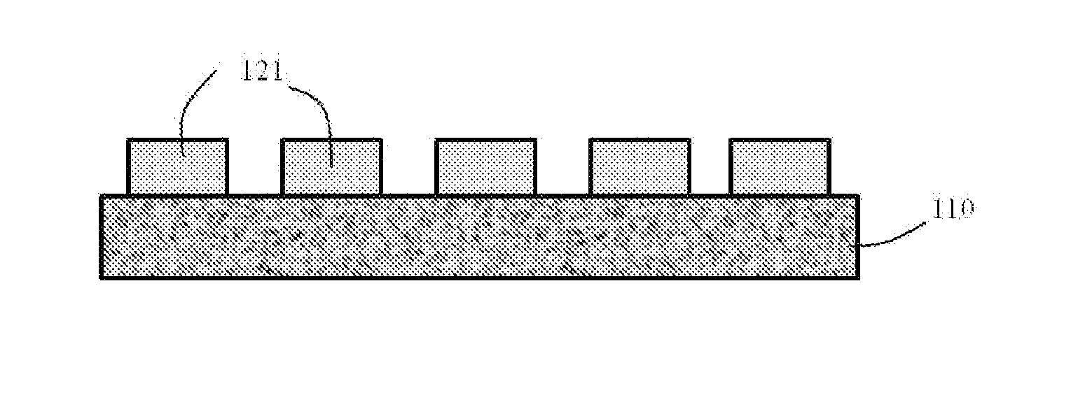
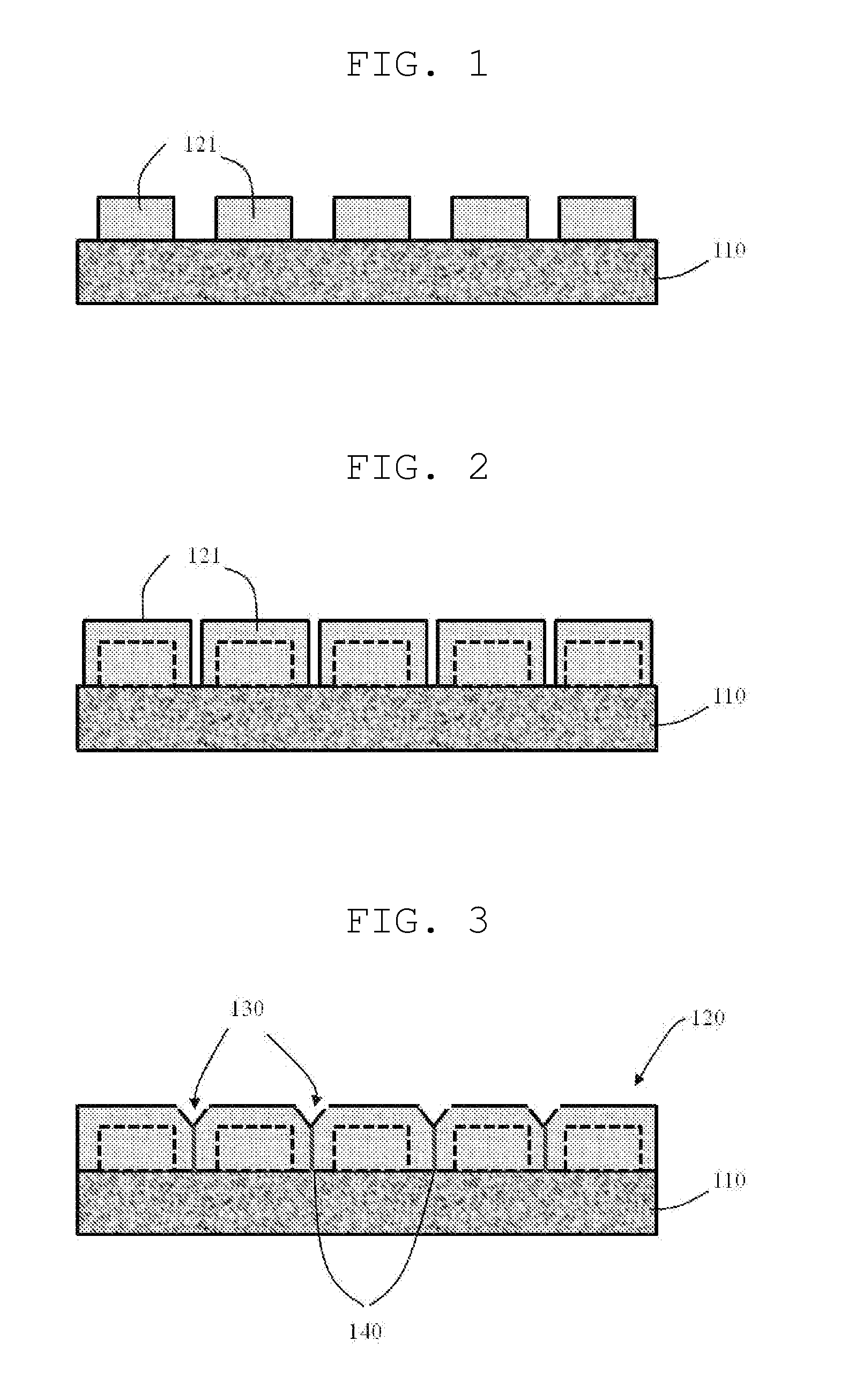
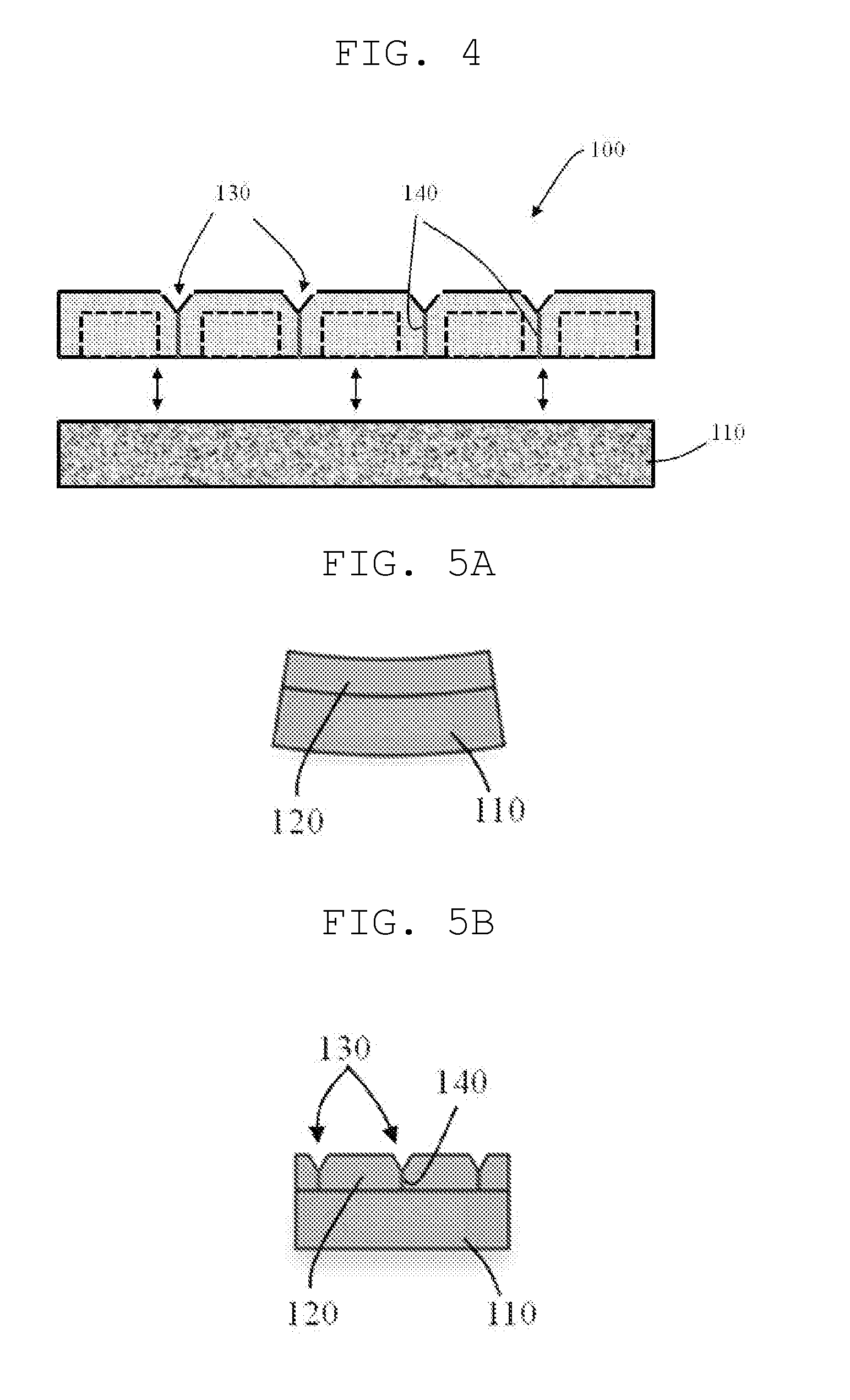
[0055]A method of manufacturing a GaN substrate according to an embodiment of the present invention is a method of manufacturing a freestanding GaN substrat...


PUM

PropertyMeasurementUnit
thicknessaaaaaaaaaa
band gap energyaaaaaaaaaa
melting pointaaaaaaaaaa

Abstract

A method of manufacturing a gallium nitride (GaN) substrate and a GaN substrate manufactured by the same. The method includes the steps of growing a GaN film on a base substrate and separating the base substrate from the GaN film. The step of growing the GaN film includes forming pits in the GaN film, the pits inducing an inversion domain boundary to be formed inside the GaN film. The GaN substrate can have a predetermined thickness with which it can be handled during layer transfer (LT) processing, and the warping of the GaN substrate can be minimized, thereby preventing cracks due to warping.

Description

CROSS REFERENCE TO RELATED APPLICATION[0001]The present application claims priority from Korean Patent Application Numbers 10-2012-0070389 and 10-2012-0147987 filed on Jun. 29, 2012 and Dec. 18, 2012, respectively, the entire contents of which application are incorporated herein for all purposes by this reference.BACKGROUND OF THE INVENTION[0002]1. Field of the Invention[0003]The present invention relates to a method of manufacturing a gallium nitride (GaN) substrate and a GaN substrate manufactured by the same, and more particularly, to a method of manufacturing a GaN substrate and a GaN substrate manufactured by the same, in which the GaN substrate can have a predetermined thickness with which it can be handled during layer transfer (LT) processing, and the warping of the GaN substrate can be minimized, thereby preventing cracks due to the warping.[0004]2. Description of Related Art[0005]Gallium nitride (Ga) is a direct transition semiconductor material having band gap energy of 3...

Claims


Application Information

Patent Timeline
Patent Type & Authority Applications(United States)
IPC IPC(8): H01L21/02H01L33/00
CPCH01L21/0254H01L33/0075C30B25/02C30B25/16C30B29/406H01L21/0237H01L21/02458H01L21/02502H01L21/02513H01L21/0262H01L21/02664
Inventor LIM, SUNGKEUNPARK, BOIKWOO, KWANGJEKIM, WOORIHANKIM, JOON HOIPARK, CHEOLMINBAE, JUNYOUNGLEE, DONGYONGLEE, WONJOCHOI, JUNSUNG
Owner SAMSUNG CORNING PRECISION MATERIALS CO LTD
Why Eureka
Try Eureka