Inspection method and system

a technology of inspection method and inspection apparatus, which is applied in the direction of measurement devices, instruments, scientific instruments, etc., can solve the problems of reducing yield, affecting the processing of defect detection, and requiring a large manufacturing cost for lsi production, so as to improve inspection accuracy, prevent unnecessary contact between replica template and resist, and increase productivity

Active Publication Date: 2014-01-02
NUFLARE TECH INC
View PDF2 Cites 20 Cited by
  • Summary
  • Abstract
  • Description
  • Claims
  • Application Information

AI Technical Summary

Benefits of technology

[0009]In the nanoimprint technology, to increase productivity, duplicate templates (replica templates) are produced using a master template as an original plate, and the replica templates are mounted and used in different nanoimprint apparatuses. The replica template is required to be produced so as to accurately correspond to the master template. Thus, high inspection accuracy is required when the replica template is inspected.
[0010]The replica template has a mesa structure in which the central portion protrudes relative to the outer circumferential portion, and a pattern is formed on the protruding portion (referred to as a mesa portion or a land portion). According to this structure, when the pattern is transferred onto a resist, the occurrence of unnecessary contact between the replica template and the resist can be prevented.

Problems solved by technology

Enhancement of yield is essential, as the manufacture of LSI requires a large manufacturing cost.
In these circumstances, a pattern defect of a mask and variation of process terms and conditions at the time of exposure and transfer constitute a major cause of reduction in the yield.
Thus, a focus depth as an allowable range of a distance between an optical system and the mask becomes deeper, and a pattern image is blurred simply by slightly changing the distance between the optical system and the mask, so that a defect detection processing is hampered.
At this time, since there is a step between the mesa portion and the other portions, there is a problem that tracking of a focus control using an automatic focus mechanism cannot be performed.
Alternatively, when the light passes through the step, although the height of a table is significantly reduced to incorporate the portion into an imaging surface, if the control using a Z table driving circuit cannot be tracked at this time, the distance between the optical system and a surface to be inspected is no longer fixed, so that a pattern image is blurred.

Method used


Image

  • Inspection method and system
  • Inspection method and system
  • Inspection method and system

Examples


embodiment 1

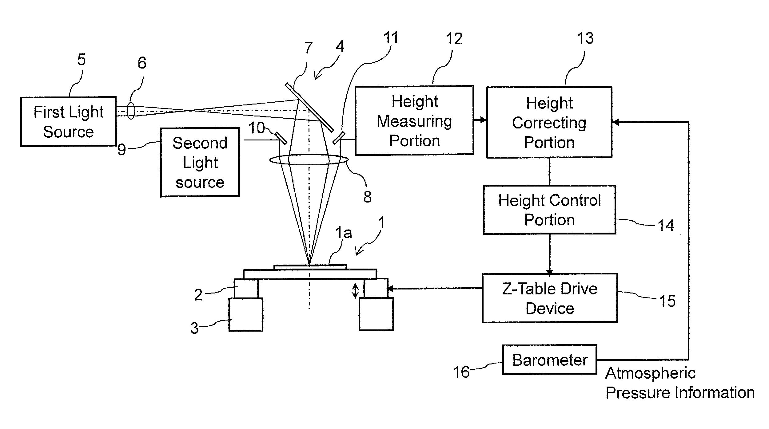
[0038]FIG. 1 is a diagram illustrating the configuration of an automatic focus mechanism according to embodiment 1.

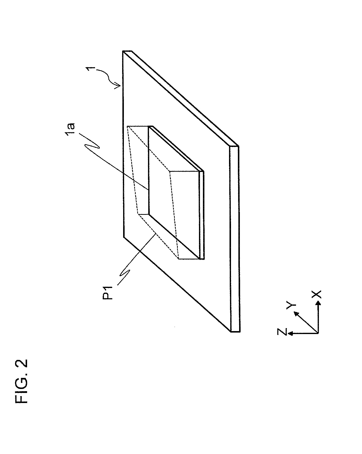
[0039]In FIG. 1, a sample 1 is mounted on a Z table 2 provided to be movable in vertical direction. The table 2 is movable in horizontal direction by a XY table 3. The sample 1 has a mesa structure in which the central portion protrudes relative to the outer circumferential portion, and a pattern to be inspected is formed on a rectangular mesa portion (referred to as a land portion) la. As the sample 1, a replica template used in the nanoimprint technology is used, for example.

[0040]An optical system 4 is disposed above the sample 1. In the optical system 4, a first light source 5 applies light for defect inspection to the sample 1. The light emitted from the first light source 5 is transmitted through a lens 6 and the direction of light is changed by a mirror 7, and, thus, is focused on the sample 1 by a lens 8. A photodiode array (not illustrated) is disposed under th...

embodiment 2

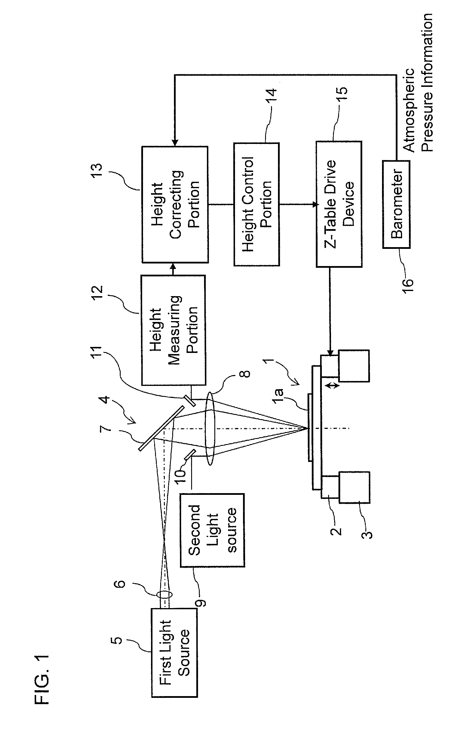
[0101]FIG. 10 is a diagram illustrating the configuration of an automatic focus mechanism according to the present embodiment. The autofocus device is suitable for inspection of a sample having a step portion on a surface to be inspected, for example, inspection of a template used in the nanoimprint lithography.

[0102]In FIG. 10, a sample 1 is mounted on a Z table 2 provided to be movable in the vertical direction. The table 2 is movable in the horizontal direction by a XY table 3. The sample 1 has a mesa structure in which the central portion protrudes relative to the outer circumferential portion, and a pattern is formed on a rectangular mesa portion la.

[0103]An optical system 4 is disposed above the sample 1. In the optical system 4, a first light source 5 applies light for defect inspection to the sample 1. The light emitted from the first light source 5 is transmitted through a lens 6 to change the direction by a mirror 7, and, thus, to be converged on the sample 1 by a lens 8. ...


PUM

PropertyMeasurementUnit
widthaaaaaaaaaa
heightaaaaaaaaaa
height mapaaaaaaaaaa

Abstract

A sample, which has a mesa portion having a pattern thereon, is placed on a Z table. Light is irradiated to the mesa portion through an optical system and light reflected by the mesa portion is received to measure a height of the mesa portion. A height map of the mesa portion is created based on a height of a corner position. A height using the height map is corrected based on a deviation of a measured value from a target value, and a temporal variation of a focal position of light irradiated to the mesa portion. An optical image of the pattern is obtained while controlling the Z table based on the corrected height of the mesa portion. The optical image is compared with a reference image and a defect is determined when a difference value between the optical image and reference image is more than a predetermined threshold value.

Description

CROSS-REFERENCE TO THE RELATED APPLICATION[0001]The entire disclosure of the Japanese Patent Application No. 2012-143975, filed on Jun. 27, 2013 including specification, claims, drawings, and summary, on which the Convention priority of the present application is based, are incorporated herein in its entirety.FIELD OF THE INVENTION[0002]This invention relates to an inspection method and an inspection apparatus and relates more specifically to an inspection method and an inspection apparatus for a sample with a mesa portion having a pattern thereon.BACKGROUND[0003]In a large scale integration (LSI), as the degree of integration and the capacity are increased, the circuit size required for a semiconductor device has been gradually narrowing. In the manufacture of the semiconductor device, a pattern is exposed and transferred onto a wafer by a reduced projection exposure apparatus generally called a stepper or scanner to form a circuit, using an original image pattern (meaning a mask o...

Claims


Application Information

Patent Timeline
Patent Type & Authority Applications(United States)
IPC IPC(8): G01N21/956G01B11/24
CPCG01N21/956G01B11/24G01N21/9501G01N21/9505G01N21/95607
Inventor INOUE, HIROMUKIKUIRI, NOBUTAKA
Owner NUFLARE TECH INC
Why Eureka
Try Eureka