Methods for fabricating integrated circuits having improved metal gate structures

a technology of metal gate structure and integrated circuit, which is applied in the direction of basic electric elements, electrical equipment, semiconductor devices, etc., can solve the problems of vt shift, leakage, and increase variability

Active Publication Date: 2014-01-02
GLOBALFOUNDRIES US INC
View PDF3 Cites 30 Cited by
  • Summary
  • Abstract
  • Description
  • Claims
  • Application Information

AI Technical Summary

Problems solved by technology

However, the use of numerous layers and multiple recessing processes to form the metal gate structures present several technical challenges in smaller technology features.
Multiple depositions and recessing of the work function metal layers and the conductive metal fill in the smaller trenches becomes increasingly difficult to control, resulting in increased variability, leakage, and Vt shift.

Method used


Image

  • Methods for fabricating integrated circuits having improved metal gate structures
  • Methods for fabricating integrated circuits having improved metal gate structures
  • Methods for fabricating integrated circuits having improved metal gate structures

Examples


Embodiment Construction

[0010]The following Detailed Description is merely exemplary in nature and is not intended to limit the various embodiments or the application and uses thereof. Furthermore, there is no intention to be bound by any theory presented in the preceding background or the following detailed description.

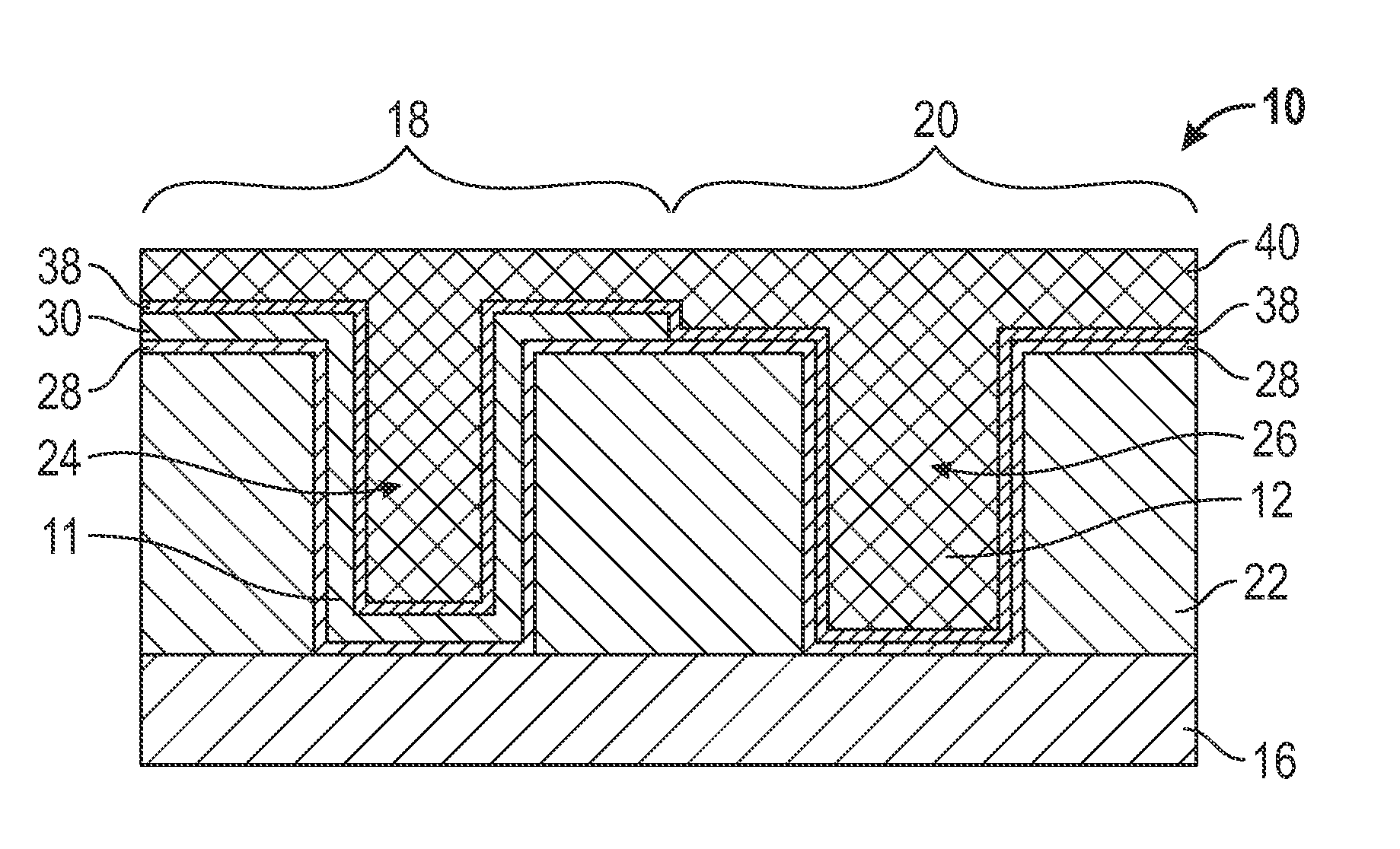
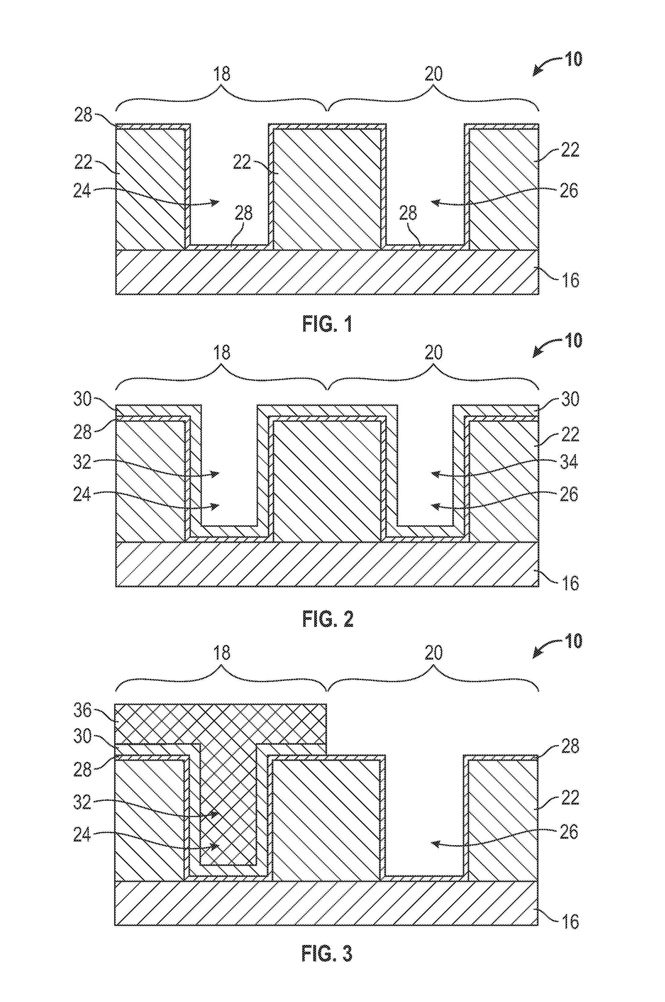
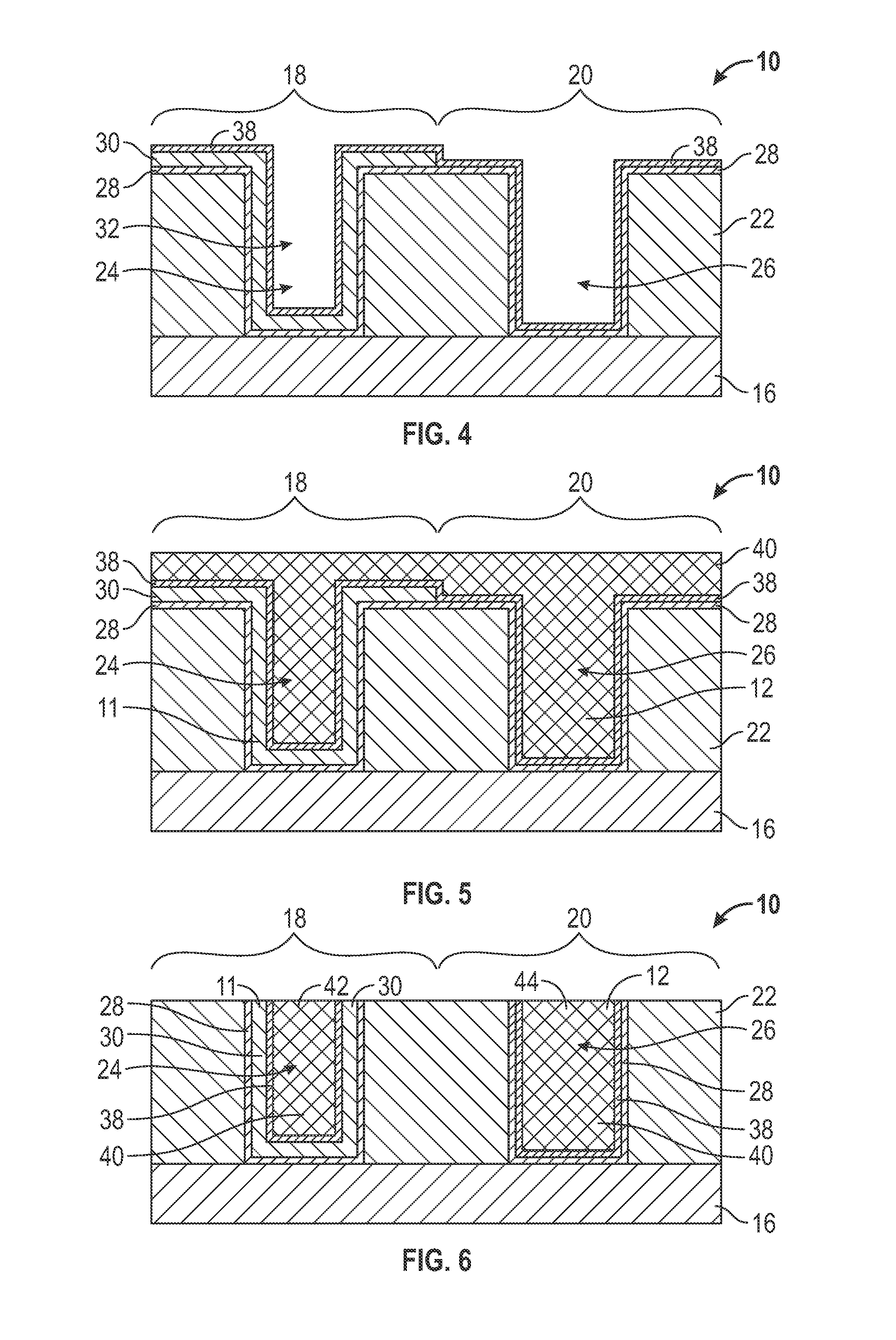
[0011]Various embodiments contemplated herein relate to methods for fabricating integrated circuits having improved metal gate structures. In accordance with one embodiment, during intermediate stages of the fabrication of an integrated circuit (IC), a NFET trench and a PFET trench are formed in a NFET region and a PFET region, respectively, of an interlayer dielectric material on a semiconductor substrate. A layer of a N-type work function metal is deposited overlying the NFET and PFET regions to partially fill the NFET and PFET trenches and define an inner cavity in the NFET trench. The N-type work function metal is a conductive work function metal that is selected from the group of titan...


PUM

PropertyMeasurementUnit
dielectric constantaaaaaaaaaa
work functionaaaaaaaaaa

Abstract

Methods for fabricating integrated circuits are provided. One method includes forming first and second FET trenches in an interlayer dielectric material on a semiconductor substrate. The first FET trench is partially filled with a first work function metal to define an inner cavity in the first FET trench. The first work function metal is a N-type work function metal or a P-type work function metal. The N-type work function metal is selected from the group consisting of titanium, tantalum, hafnium, ytterbium silicide, erbium silicide, and titanium silicide. The P-type work function metal is selected from the group consisting of cobalt, nickel, and tungsten silicide. The inner cavity and the second FET trench are filled with a second work function metal to form corresponding metal gate structures. The second work function metal is the other of the N-type work function metal or the P-type work function metal.

Description

TECHNICAL FIELD[0001]The technical field relates generally to methods for fabricating integrated circuits, and more particularly relates to methods for fabricating integrated circuits with improved metal gate structures.BACKGROUND[0002]Transistors such as metal oxide semiconductor field effect transistors (MOSFETs) or simply field effect transistors (FETs) or MOS transistors are the core building blocks of the vast majority of semiconductor integrated circuits (ICs). A FET includes source and drain regions between which a current can flow through a channel under the influence of a bias applied to a gate electrode that overlies the channel. The ICs are usually formed using both P-channel FETs (PMOS transistors or PFETs) and N-channel FETs (NMOS transistors or NFETs) and the IC is then referred to as a complementary MOS or CMOS circuit. Some semiconductor ICs, such as high performance microprocessors, can include millions of FETs. For such ICs, decreasing transistor size and thus incr...

Claims


Application Information

Patent Timeline
Patent Type & Authority Applications(United States)
IPC IPC(8): H01L21/28
CPCH01L21/28079H01L21/28097H01L29/495H01L29/4975H01L29/66545H01L21/823842
Inventor HOON, KIM
Owner GLOBALFOUNDRIES US INC
Why Eureka
Try Eureka