Conductive substrate and touch screen having same

a technology of conductive substrate and touch screen, which is applied in the direction of circuit optical details, instruments, other domestic objects, etc., can solve the problems of reducing the legibility of users, increasing the cost of ito film, increasing the difficulty of application to enlargement while manufacturing is performed, etc., to prevent a reduction in display image quality, excellent conductivity, and reduce reflective diffraction.

Active Publication Date: 2014-01-16
LG ELECTRONICS INC +1
View PDF6 Cites 14 Cited by
  • Summary
  • Abstract
  • Description
  • Claims
  • Application Information

AI Technical Summary

Benefits of technology

[0022]The conducting substrate and the touch screen comprising the same according to the present invention may not block a view, have excellent conductivity, reduce a reflective diffraction phenomenon due to a point light source, and prevent a reduction in display image quality by a moire phenomenon. In addition, since the electric conducting pattern according to the present invention can be formed by various methods such as an indirect printing method, a photolithography method, a photography method, a method using a hard mask, or a sputtering method

Problems solved by technology

However, since most of the transparent conducting films has high resistance of 150 ohm/square or more, sensitivity is reduced in enlargement, and when the touch screen is manufactured by using the same, there are a complexity that a patterning process of ITO and a patterning process of an electrode of a metal trace portion are sequentially performed by a process such as photolithography and a problem that a cost of an ITO film is rapidly increased as a size of a screen is increased, such that there are an increase in manufacturing cost and difficulty in application to enlargement while manufacturing is performed.
In this case, the reflective diffraction phenomenon means that when the point light source such as sunlight or interior LED radiates light on a surface where the metal pattern of the display is provided, in the case

Method used


Image

  • Conductive substrate and touch screen having same
  • Conductive substrate and touch screen having same
  • Conductive substrate and touch screen having same

Examples


example

Examples 1 to 2

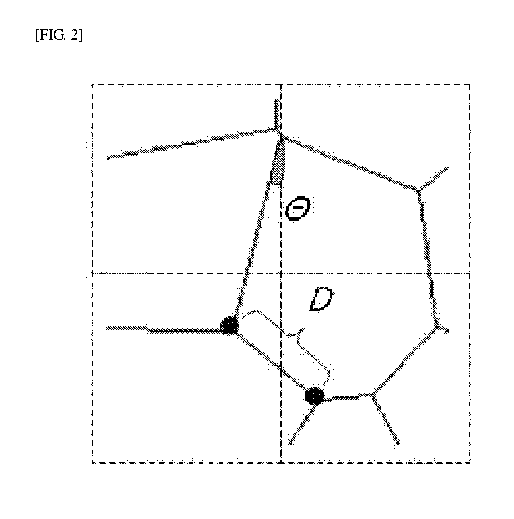
[0124]One of the methods of differentiating an irregular pattern type of electric conducting pattern according to the present invention from a general regular pattern having randomness of 0 is a method of confirming the number of vertexes of the line in the unit area. That is, the case where all distances of the vertexes constituting the closed figure are not the same as each other and the number of vertexes of a basic figure constituting the pattern is about two times larger than the number of vertexes of another figure formed by connecting the centers of masses of the closed figures may be defined as the irregular pattern type of electric conducting pattern according to the present invention.

[0125]This difference can be seen by, as described in the following Tables 2 and 3, comparing the numbers of polygons according to randomness existing in the unit area (3.5 cm×3.5 cm) of the known regular pattern and the electric conducting pattern according to the present inve...

example 3

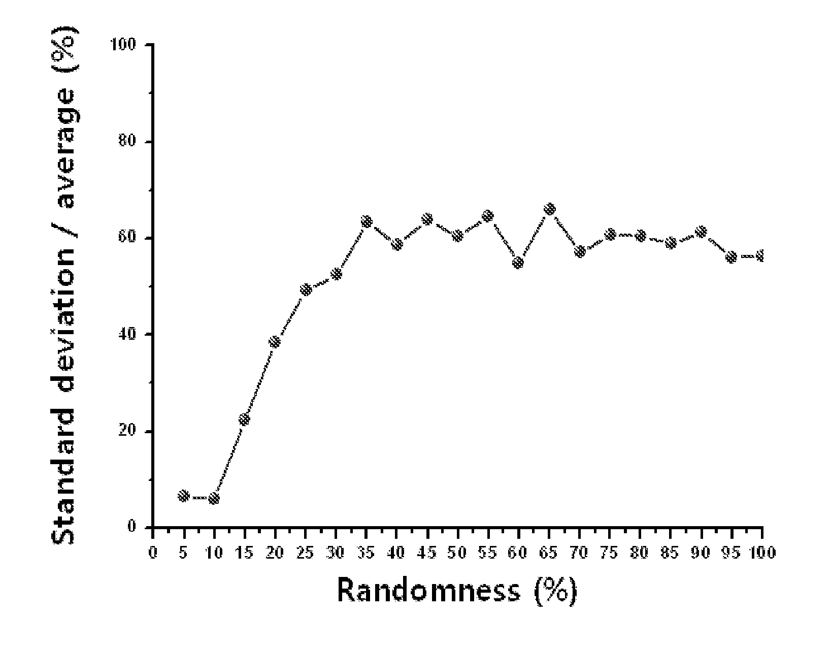
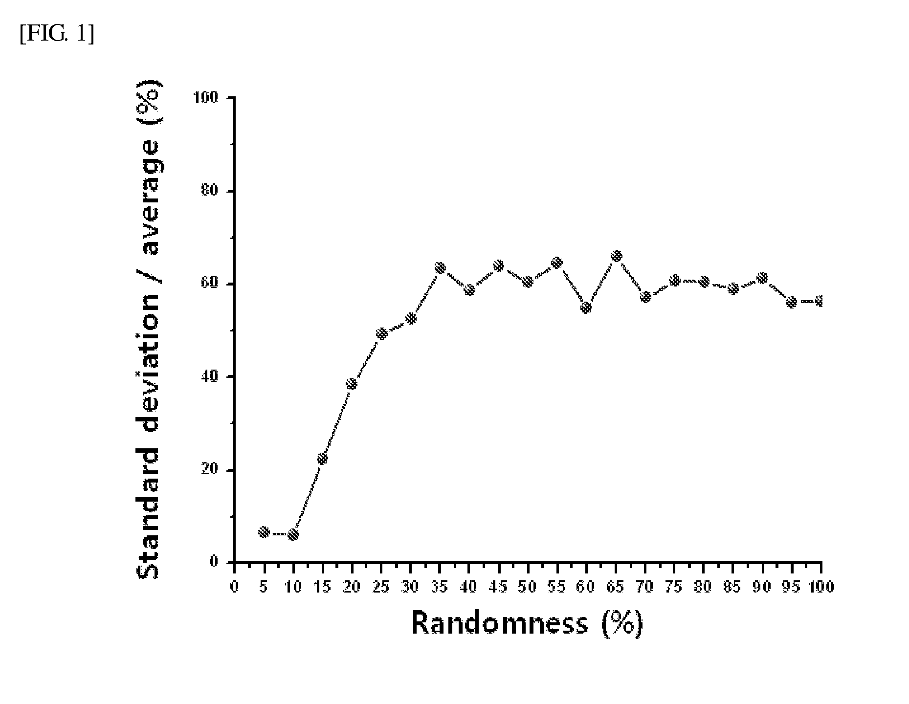
[0127]Further, in the present invention, the relationship of the distances between the vertexes and the number distribution of components of the sides constituting the electric conducting pattern in the unit area according to the angle were confirmed. As a result, the results of the following Table 4 and FIG. 3 could be obtained, and from the results thereof, it could be confirmed that the numbers of lines according to the angle were relatively uniformly distributed in the case where the randomness was 70% or more.

TABLE 4RandomnessAngle010%30%50%70%100%0 or more to49702501207913961070885less than 1010 or more to00414829818821less than 2020 or more to003292710852less than 3030 or more to07427638666843less than 4040 or more to0243215901045868761less than 5050 or more to015434616710825less than 6060 or more to021312653818less than 7070 or more to00437818833803less than 8080 or more to02501207314561101847less than 9090 or more to49702475202814421093814less than 100100 or more to00432790...

example 4

[0128]In the present invention, whether the moire according to the randomness occurs or not was confirmed (area having the size of 3.5 cm×3.5 cm) based on the results thereof, and the results are shown in the following FIG. 8. That is, in the case where randomness is 70% or more, it was confirmed that the moire avoidance effect was exhibited over the full range of the moire.

[0129]The conducting substrate and the touch screen comprising the same according to the present invention may not block a view, have excellent conductivity, reduce a reflective diffraction phenomenon by a point light source, and prevent a reduction in display image quality by a moire phenomenon. In addition, since the electric conducting pattern according to the present invention can be formed by various methods such as an indirect printing method, a photolithography method, a photography method, a method using a hard mask, or a sputtering method after a desired pattern is previously set, the process is easily p...


PUM


Abstract

The present invention relates to a conducting substrate and a touch screen comprising the same, and the conducting substrate according to the present invention comprises a board, and an electric conducting pattern provided on at least one surface of the board, wherein the electric conducting pattern comprises a border structure of closed figures continuously connected and does not comprise the closed figures having the same shape in a predetermined unit area (1 cm×1 cm), and the number of vertexes of the closed figures is different from the number of vertexes of quadrangles having the same number as the closed figures.

Description

TECHNICAL FIELD [0001]This application claims priority from Korean Patent Application No. 10-2011-0027832 filed on Mar. 28, 2011 in the KIPO, the disclosure of which is incorporated herein by reference in its entirety.[0002]The present invention relates to a conducting substrate and a touch screen comprising the same.BACKGROUND ART [0003]In general, a display device refers to monitors for a TV or a computer as a whole, and comprises a display diode forming an image and a case supporting the display diode.[0004]Examples of the display diode may comprise a plasma display panel (PDP), a liquid crystal display (LCD), an electrophoretic display, a cathode-ray tube (CRT), an OLED display and the like. An RGB pixel pattern for implementing an image and an additional optical filter may be provided in the display diode.[0005]Meanwhile, relating to a display device, as the spread of smart phones, tablet PCs, and IPTVs is accelerated, a demand for a touch function that uses human hands as a di...

Claims


Application Information

Patent Timeline
IPC IPC(8): G02F1/1333H05K1/02
CPCG02F1/13338H05K1/0274G06F2203/04103G06F2203/04112G06F3/0443G06F3/0446B32B2457/208G06F3/041
Inventor HWANG, JI YOUNGHWANG, IN-SEOKLEE, SEUNG HEONCHUN, SANG KISON, YONG GOOKOO, BEOM MOSEONG, JIEHYUNKIM, JOO YEONPARK, JE SEOB
Owner LG ELECTRONICS INC
Why Eureka
Try Eureka