Compositions and methods for selective polishing of silicon nitride materials

a technology of silicon nitride and composition, applied in the direction of electrical equipment, chemical equipment and processes, other chemical processes, etc., can solve the problems of poor manufacturing yield, unacceptable polishing rate, and inability to selectivity for the removal of insulator materials used in wafer manufacturing, and achieve low polysilicon removal rate and high silicon nitride removal rate

Active Publication Date: 2014-01-16
CMC MATERIALS INC
View PDF4 Cites 13 Cited by
  • Summary
  • Abstract
  • Description
  • Claims
  • Application Information

AI Technical Summary

Benefits of technology

[0016]The compositions of the invention provide the advantage of high silicon nitride removal rates,

Problems solved by technology

Although known CMP slurry compositions typically are suitable for limited purposes, many conventional compositions exhibit unacceptable polishing rates and correspondingly unacceptable selectivity for removal of insulator materials used in wafer manufacture.
In addition, many known po

Method used


Image

  • Compositions and methods for selective polishing of silicon nitride materials

Examples


example 1

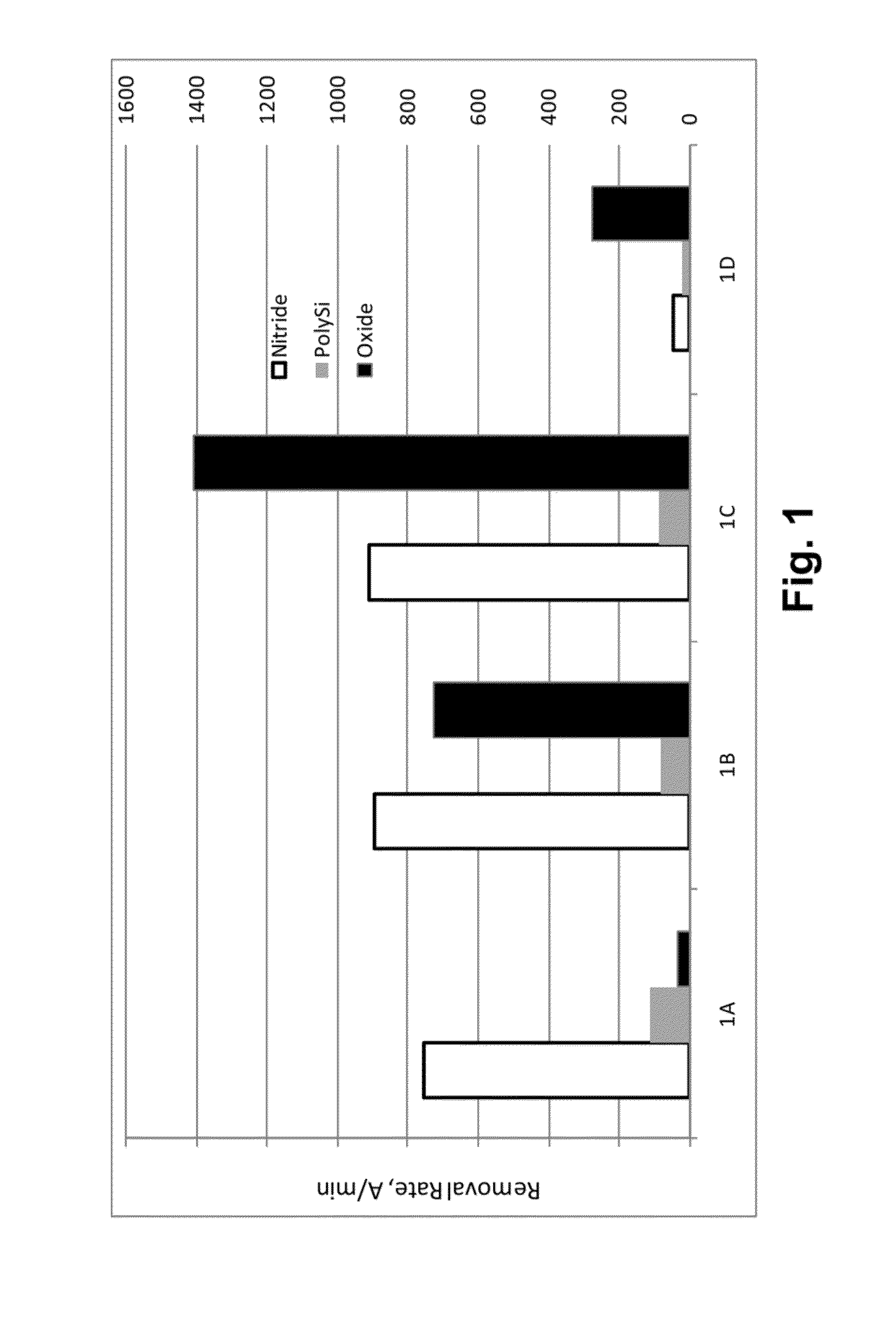
[0043]This example illustrates the effect of cationic polymers and a non-polymeric UNH compound on removal of silicon nitride, polysilicon, and silicon oxide.

[0044]Polishing compositions were used to separately chemically-mechanically polish silicon nitride, silicon oxide, and polysilicon blanket wafers on a Mirra 200 mm CMP apparatus with a D100 polishing pad. Each of the polishing compositions comprised an aqueous slurry of about 0.2 wt % calcined ceria (Advanced Nano Products Co., Ltd., “ANP”, average particle size of about 100 nm), in deionized water at a pH of about 4. Additional components of the CMP compositions are shown in Table 1, in which “Quat” refers to poly(methacryloyloxyethyl trimethylammonium chloride) from Alco Chemical (Alco 4773); p(4-PV) refers to poly(4-vinylpyridine); TMDP refers to 4,4′-trimethylenedipyridine; and PEG 1450 refers to poly(ethylene glycol) having a number average molecular weight of about 1450 Daltons.

TABLE 1ExampleQuat, ppm4-PVP, ppmTMDP, ppmP...

example 2

[0047]Evaluations of additional formulations lacking poly(4-vinylpyridine) were performed on a Mirra polisher with a POLITEX® pad, at a down pressure of about 3 psi, a polishing head speed (HS) of about 101 rpm, a platen speed (PS) of about 100 rpm, and a slurry flow rate of about 150 mL / min. Each of the tested compositions were prepared with calcined ceria in deionized water as in Example 1 and had a pH of about 4. The concentration of the various components, of the formulations are shown in Table 3, while the observed polishing rates for nitride, polysilicon and oxide, in A / min are shown in Table 4. In each of Tables 3 and 4, the abbreviations used are the same as those used in Example 1.

TABLE 3CeriaTMDPQuatPEG 1450Examplewt %ppmppmppm2A0.20002B0.275158002C0.250308002D0.250158002E0.25008002F0.27508002G0.2100308002H0.210008002I0.275308002J0.2100158002K0.375158002L0.17515800

TABLE 4ExampleNitride RRPolySi RROxide RR2A14218020122B10196617572C11555715882D10286619032E72210015192F7787215...

example 3

[0049]This example illustrates the effect of including an EO / PO block copolymer in CMP compositions of the invention, in addition to PEG 1450. Evaluations were performed on a Mirra polisher with a D100 pad, at a down pressure of about 3 psi, a polishing head speed (HS) of about 101 rpm, a platen speed (PS) of about 100 rpm, and a slurry flow rate of about 150 mL / min. Each of the tested compositions were prepared with calcined ceria in deionized water as in Example 1 and had a pH of about 4 except for Examples 3K and 3L, which had a pH of about 2.3. The concentration of the various components of the formulations are shown in Table 5, while the observed polishing rates for nitride, polysilicon and oxide, in A / min are shown in Table 6. In each of Tables 5 and 6, L31 refers to PLURONIC® L31 surfactant (BASF), and the remaining abbreviations are the same as those used in Example 1.

TABLE 5L31CeriaTMDPQuatPEG 1450Exampleppmwt %ppmppmppm3A5000.2100708003B5000.2100508003C5000.2140508003D5000...


PUM


Abstract

The present invention provides an acidic aqueous polishing composition suitable for polishing a silicon nitride-containing substrate in a chemical-mechanical polishing (CMP) process. The composition, at point of use, preferably comprises about 0.01 to about 2 percent by weight of at least one particulate ceria abrasive, about 10 to about 1000 ppm of at least one non-polymeric unsaturated nitrogen heterocycle compound, 0 to about 1000 ppm of at least one cationic polymer, optionally, 0 to about 2000 ppm of at least one polyoxyalkylene polymer, and an aqueous carrier therefor. The cationic polymer preferably is selected from a poly(vinylpyridine) polymer, a quaternary ammonium-substituted acrylate polymer, a quaternary ammonium-substituted methacrylate polymer, or a combination thereof. Methods of polishing substrates and of selectively removing silicon nitride from a substrate in preference to removal of polysilicon using the compositions are also provided.

Description

FIELD OF THE INVENTION[0001]This invention relates to polishing compositions and methods. More particularly, this invention relates to methods for polishing silicon nitride-containing substrates and compositions therefor.BACKGROUND OF THE INVENTION[0002]A semiconductor wafer for integrated circuits typically includes a substrate, such as silicon or gallium arsenide, on which a plurality of transistors have been formed. Transistors are chemically and physically connected to the substrate by patterning regions in the substrate and layers on the substrate. The transistors and layers are separated by interlevel dielectrics (ILDs), comprised primarily of some form of silicon oxide (SiO2). The transistors are interconnected through the use of well-known multilevel interconnects. Typical multilevel interconnects are comprised of stacked thin-films consisting of one or more of the following materials: titanium (Ti), titanium nitride (TiN), tantalum (Ta), aluminum-copper (Al—Cu), aluminum-si...

Claims


Application Information

Patent Timeline
IPC IPC(8): H01L21/306C09K13/00
CPCC09G1/02C09K3/1409C09K3/1463H01L21/31053H01L21/30625H01L21/31116H01L21/32139
Inventor WARD, WILLIAM
Owner CMC MATERIALS INC
Why Eureka
Try Eureka