Display device
a display device and transistor technology, applied in non-linear optics, instruments, optics, etc., can solve the problems of deteriorating display quality and lowering reliability of display devices, and achieve the effect of suppressing the deterioration of display quality of display devices including transistors, reducing reliability, and increasing reliability
- Summary
- Abstract
- Description
- Claims
- Application Information
AI Technical Summary
Benefits of technology
Problems solved by technology
Method used
Image

Examples
embodiment 1
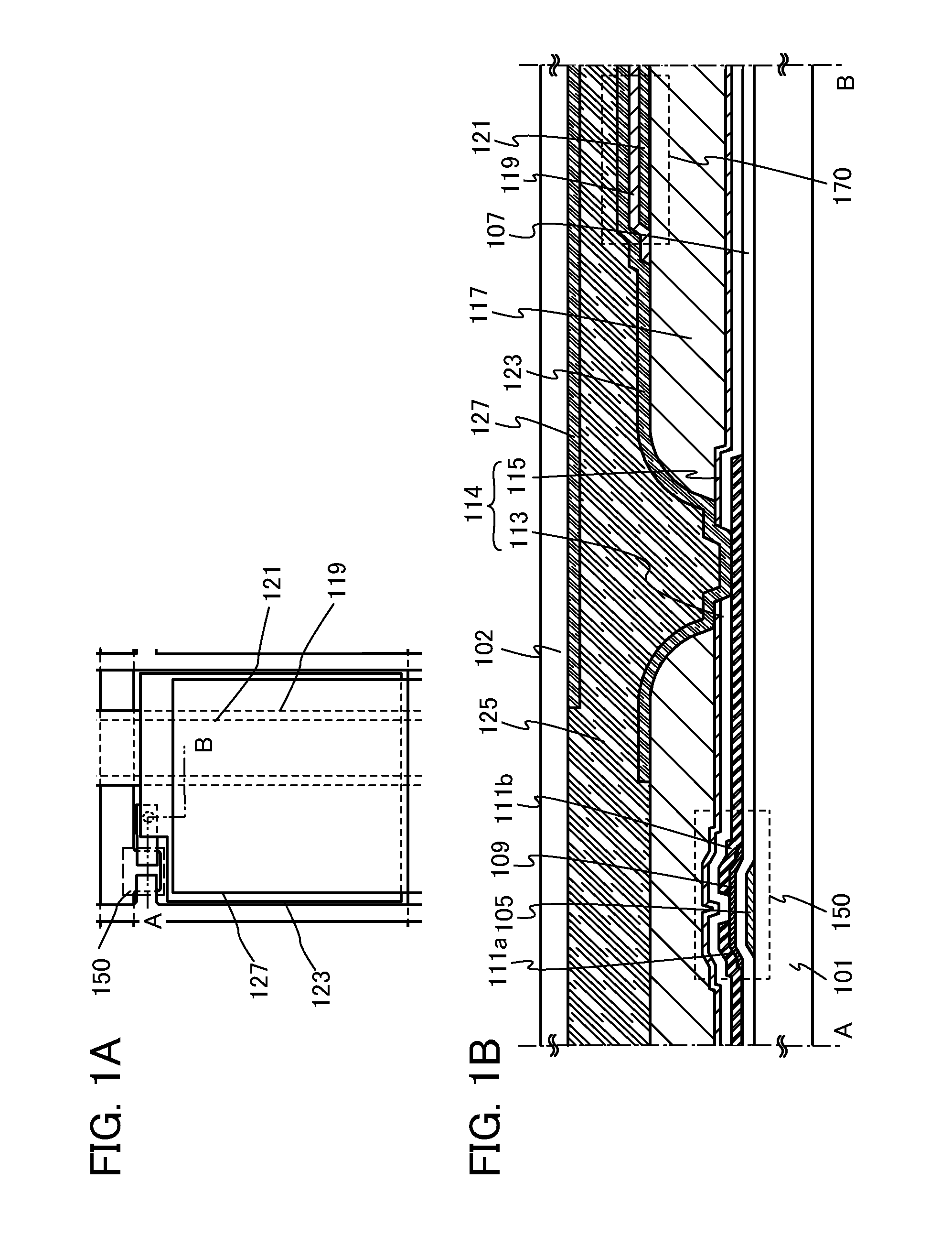
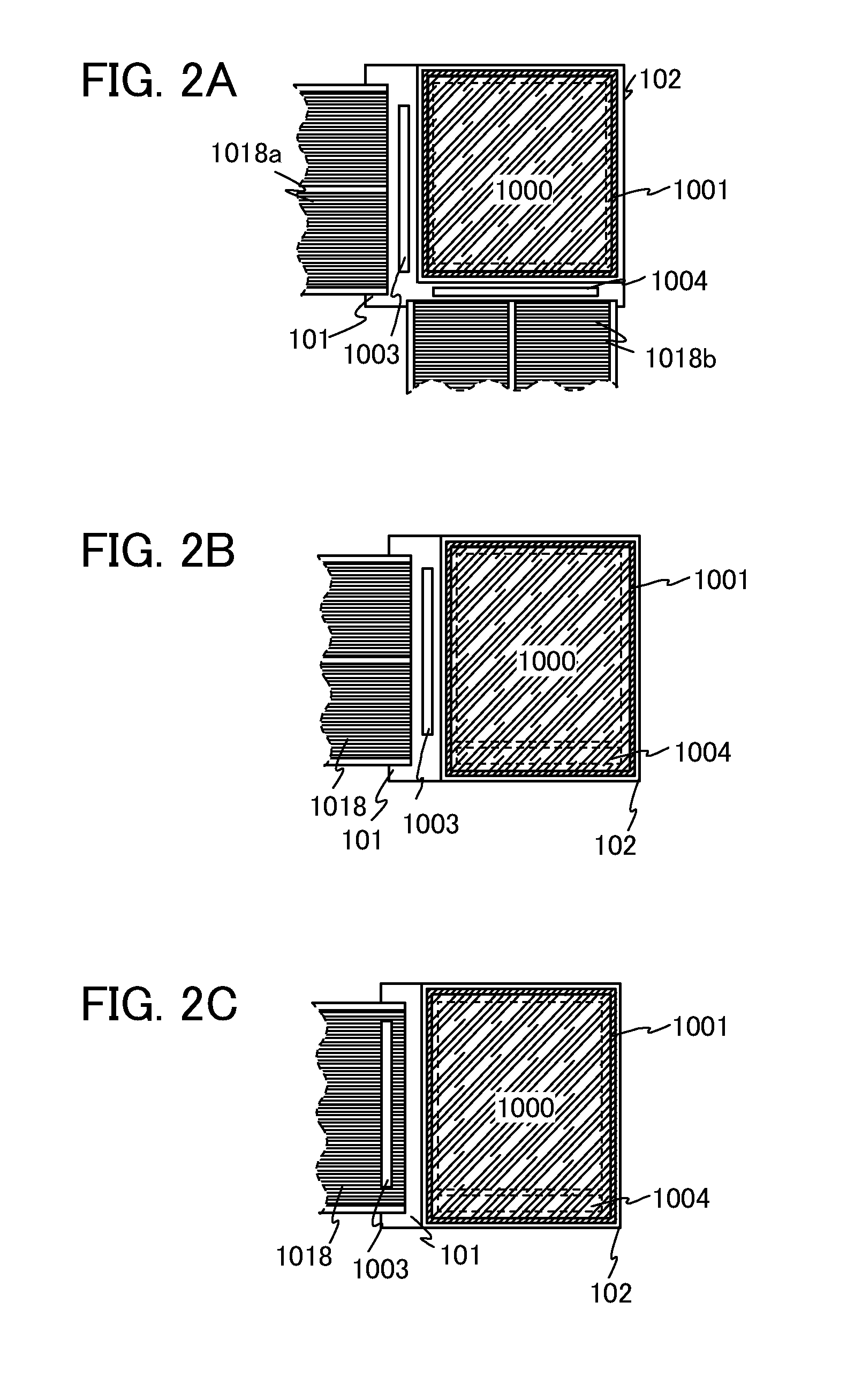
[0039]In this embodiment, a display device of one embodiment of the present invention will be described with reference to the drawings. FIGS. 2A to 2C are top views each illustrating a display device of this embodiment.
[0040]FIG. 2A is a top view illustrating a display device of one embodiment of the present invention. In FIG. 2A, a sealant 1001 is provided so as to surround a pixel portion 1000 provided over a first substrate 101, and sealing is performed using a second substrate 102. In FIG. 2A, a scan line driver circuit 1004 and a signal line driver circuit 1003 each of which is formed using a single crystal semiconductor film or a polycrystalline semiconductor film over a substrate separately prepared are mounted in a region different from the region surrounded by the sealant 1001 over the first substrate 101. Various signals and potentials are supplied from flexible printed circuits (FPCs) 1018a and 1018b to the signal line driver circuit 1003, the scan line driver circuit 100...
embodiment 2
[0182]In this embodiment, an image sensor that can be used in combination with any of the display devices described in the above embodiment is described.
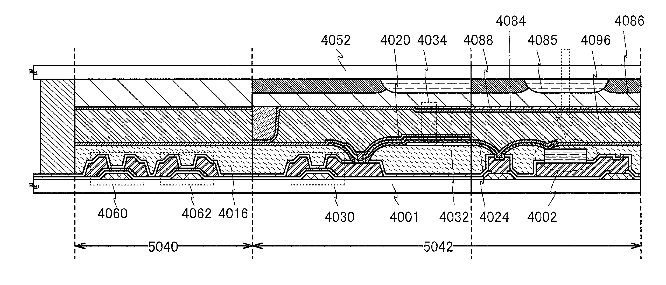
[0183]An example of a display device with an image sensor is illustrated in FIG. 6A. FIG. 6A illustrates an equivalent circuit of a pixel of the display device with an image sensor.
[0184]One electrode of a photodiode element 4002 is electrically connected to a reset signal line 4058, and the other electrode of the photodiode element 4002 is electrically connected to a gate electrode of a transistor 4040. One of a source electrode and a drain electrode of the transistor 4040 is electrically connected to a power supply potential (VDD), and the other of the source electrode and the drain electrode of the transistor 4040 is electrically connected to one of a source electrode and a drain electrode of a transistor 4056. A gate electrode of the transistor 4056 is electrically connected to a gate selection line 4057, and the other of the so...
embodiment 3
[0200]In this embodiment, an example of a tablet terminal using a display device of one embodiment of the present invention is described.
[0201]FIGS. 7A and 7B illustrate a foldable tablet terminal. FIG. 7A illustrates the tablet terminal which is unfolded. The tablet terminal includes a housing 8630, and a display portion 8631a, a display portion 8631b, a display mode switch 8034, a power switch 8035, a power-saving mode switch 8036, a clasp 8033, and an operation switch 8038 which are provided on the housing 8630.
[0202]The whole or part of the display portion 8631a can function as a touch panel and data can be input when a displayed operation key is touched. For example, the display portion 8631a can display keyboard buttons in the whole region to function as a touch panel, and the display portion 8631b may be used as a display screen.
[0203]Like the display portion 8631a, the whole or part of the display portion 8631b can function as a touch panel.
[0204]Further, a touch panel regio...
PUM
 Abstract
Description
Claims
Application Information
 - R&D
- Intellectual Property
- Life Sciences
- Materials
- Tech Scout
- Unparalleled Data Quality
- Higher Quality Content
- 60% Fewer Hallucinations
Browse by: Latest US Patents, China's latest patents, Technical Efficacy Thesaurus, Application Domain, Technology Topic, Popular Technical Reports.
© 2025 PatSnap. All rights reserved.Legal|Privacy policy|Modern Slavery Act Transparency Statement|Sitemap|About US| Contact US: help@patsnap.com