Bonding apparatus and bonding tool cleaning method

a technology of bonding apparatus and cleaning method, which is applied in the direction of soldering apparatus, manufacturing tools,auxillary welding devices, etc., can solve the problems of unexpectedly large balls, increase in thickness, and decrease in bonding strength, so as to reduce the diameter of the deformed ball bonded, prevent shortening between adjacent pads, and reduce the effect of bonding strength

Inactive Publication Date: 2014-02-06
SHINKAWA CO LTD
View PDF8 Cites 11 Cited by
  • Summary
  • Abstract
  • Description
  • Claims
  • Application Information

AI Technical Summary

Benefits of technology

[0042]In accordance with the present invention, the residual energy in the bonding tool is prohibited from having an impact on the free-air ball formed in the wire, whereby the

Problems solved by technology

However, the inventions disclosed in Japanese Unexamined Patent Application Publication Nos. 2008-21943 and 2008-218789 may suffer from various inconveniences such as electrical shorting between adjacent pads resulting from the diameter of deformed balls bonded at bonding positions exceeding a predetermined size during a bonding operation after cleaning the tip and the side surface of the bonding tool and/or may undergo a reduction in the bonding stre

Method used


Image

  • Bonding apparatus and bonding tool cleaning method
  • Bonding apparatus and bonding tool cleaning method
  • Bonding apparatus and bonding tool cleaning method

Examples


embodiment

[0075]A preferred embodiment of the present invention will now be described in line with the following flow.

1. Configuration of a Bonding Apparatus According to the Embodiment

(1) Overall Configuration

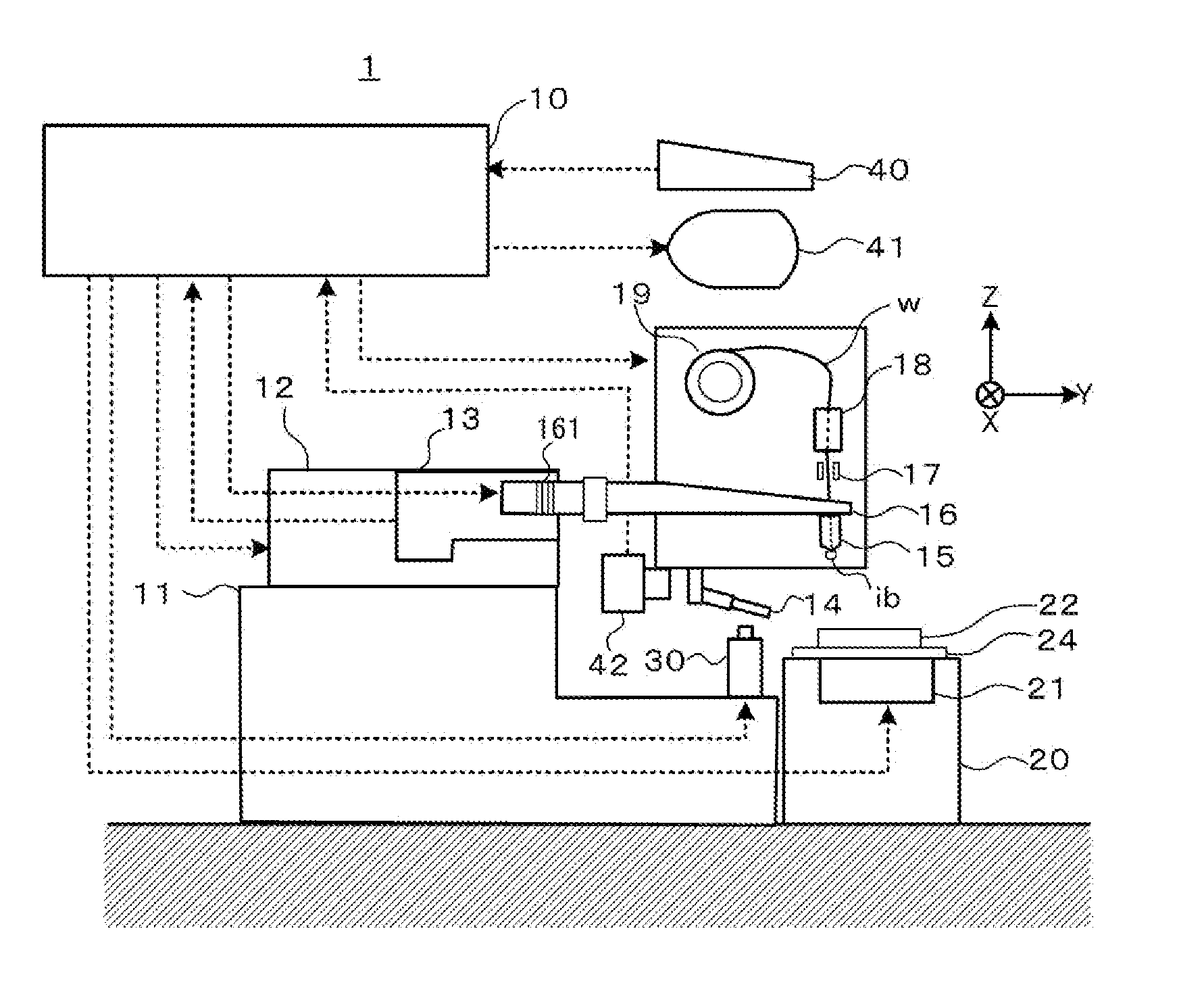
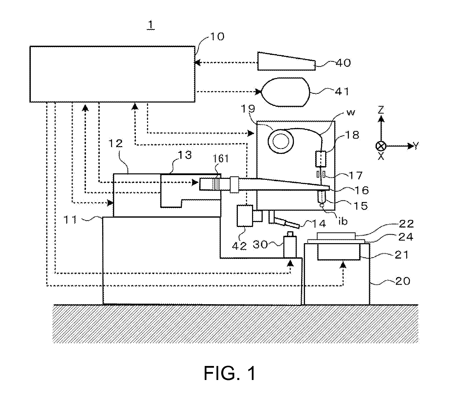
[0076]FIG. 1 is a configuration diagram of the bonding apparatus according to the embodiment.

[0077]As shown in FIG. 1, the bonding apparatus 1 according to the embodiment includes a controller 10, a base 11, an XY table 12, a bonding head 13, a torch electrode 14, a capillary 15, a bonding arm 16, a wire clamper 17, a wire tensioner 18, a rotary spool 19, a feeder 20, a heater 21, a plasma irradiation device 30, an operation unit 40, a display 41, and a camera 42.

[0078]In the following embodiments, a plane parallel to a bonding target semiconductor die or lead frame is defined as XY plane and the direction perpendicular to the XY plane is defined as Z direction. The tip position of the capillary 15 is identified with a spatial coordinate (X, Y, Z) represented by an X coordinate, a Y coo...

first embodiment

(1) First Embodiment

[0181]FIG. 10 is a flow chart illustrating a bonding tool cleaning method according to the first embodiment to which the first solution is applied. At the beginning, the cleaning flag indicating that it is immediately after the cleaning process is reset.

[0182]In step S10, a preparation is made for a bonding process. Correspondingly to operations on the operation unit 40 by the operator as mentioned above, the controller 10 records the movement trajectory of the capillary 15. When the semiconductor die 22 die bonded to the lead frame 24 is placed on the feeder 20, the controller 10 provides a control signal to heat the heater 21 to a predetermined temperature.

[0183]In step S11, after waiting for an instruction for starting the bonding process (NO), when the bonding process starting instruction is made (YES), the process goes to step S12 and the controller 10 determines whether or not the cleaning timing has come. The cleaning timing is preset as an adequate freque...

second embodiment

(2) Second Embodiment

[0193]FIG. 11 is a flow chart illustrating a bonding tool cleaning method according to the second embodiment to which the second solution is applied.

[0194]In step S10, a preparation is made for a bonding process. Correspondingly to operations on the operation unit 40 by the operator as mentioned above, the controller 10 records the movement trajectory of the capillary 15. When the semiconductor die 22 die bonded to the lead frame 24 is placed on the feeder 20, the controller 10 provides a control signal to heat the heater 21 to a predetermined temperature.

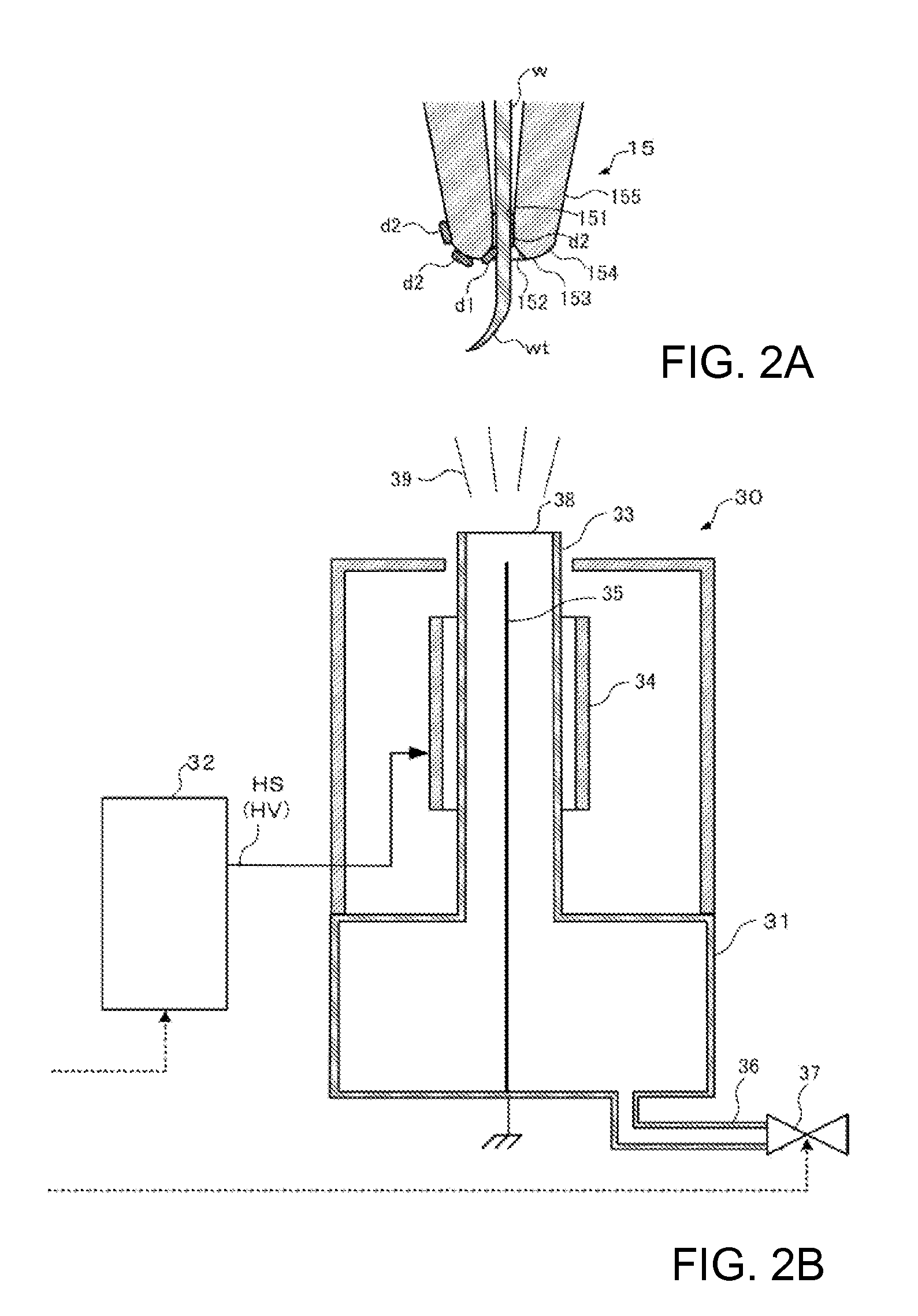
[0195]In step S11, after waiting for an instruction for starting the bonding process (NO), when the bonding process starting instruction is made (YES), the process goes to step S13 and the controller 10 performs the ball forming step (a). The controller 10 generates spark between the torch electrode 14 and the wire tail “wt” and, with the heat of the spark, forms a ball “fab” at the tip of the wire “w”.

[0196]Th...


PUM

PropertyMeasurementUnit
Diameteraaaaaaaaaa
Energyaaaaaaaaaa

Abstract

In wire bonding in which a bonding tool is cleaned through plasma irradiation, the plasma application to a wire and therefore the formation of an unexpectedly large-sized ball in the following bonding operation is prevented. The cleaning of the bonding tool through plasma irradiation is followed by dummy bonding, the bonding tool is cleaned with a ball formed thereon, or a prohibition period is provided during which ball forming is prohibited until the energy of plasma attenuates after the bonding tool is cleaned to prevent the plasma irradiation from having an impact on the bonding operation so that the ball cannot have an increased diameter.

Description

BACKGROUND OF THE INVENTION[0001]1. Technical Field[0002]The present invention relates to a bonding apparatus having a feature of cleaning a tip portion of a bonding tool and also to a bonding tool cleaning method.[0003]2. Related Art[0004]In semiconductor device manufacturing processes, a bonding apparatus is used to connect pads on a semiconductor die placed on a lead frame and leads on the lead frame. Such a bonding apparatus includes a bonding tool called wedge tool or capillary and is arranged to use a wire inserted through the bonding tool to bond the pads on the semiconductor die and the leads on the lead frame.[0005]The more the number of wires connected, the more foreign matters adhere to a tip portion of the bonding tool and the more inconveniences are likely to occur in bonding. In order to reduce such inconveniences, there has been developed a technique for cleaning foreign matters adhering to the tip portion of the bonding tool.[0006]Japanese Unexamined Patent Applicati...

Claims


Application Information

Patent Timeline
IPC IPC(8): B23K3/08
CPCB23K3/08H01L24/78H01L2224/49175H01L2224/78301H01L2224/48091H01L2224/48247H01L2224/48465H01L2224/85181H01L2924/01029H01L24/48H01L24/49H01L2224/7801H01L2224/85205H01L2924/3011H01L2224/451H01L2224/45147H01L2224/45139H01L2924/30111H01L2224/45124H01L2224/45144H01L2924/00014H01L24/45H01L2224/05554H01L2224/85132H01L2924/19107H01L24/85H01L2224/78251H01L2924/00011H01L2924/00012H01L2924/00H01L2924/00015H01L2224/05599H01L2924/01049B08B7/0035B08B7/028B23K20/004H01L2224/78343H01L2224/7855H01L2224/78611H01L2224/85345
Inventor MAEDA, TORUUTANO, TETSUYA
Owner SHINKAWA CO LTD
Why Eureka
Try Eureka