Image processing device, image processing method, image processing program, and virtual microscope system

a technology of image processing and microscope, applied in the field of image processing devices, image processing methods, image processing programs, etc., can solve problems such as errors along with modeling, refraction and scattering, and inability to accurately estimate thickness

Inactive Publication Date: 2014-02-13
OLYMPUS CORP
View PDF2 Cites 3 Cited by
  • Summary
  • Abstract
  • Description
  • Claims
  • Application Information

AI Technical Summary

Problems solved by technology

Dyes are dispersed in a sample, and thus the concept of thickness may not be accurate.
However, in an actual stained sample, refraction and scattering can both occur.
Therefore, when attenuation of light due to the stained sample is modeled only by the Lambert-Beer law, errors may occur along with the modeling.
However, it is quite difficult to construct a model including refraction or scattering in biological specimens, and doing so is infeasible in actual application.

Method used


Image

  • Image processing device, image processing method, image processing program, and virtual microscope system
  • Image processing device, image processing method, image processing program, and virtual microscope system
  • Image processing device, image processing method, image processing program, and virtual microscope system

Examples


embodiment 1

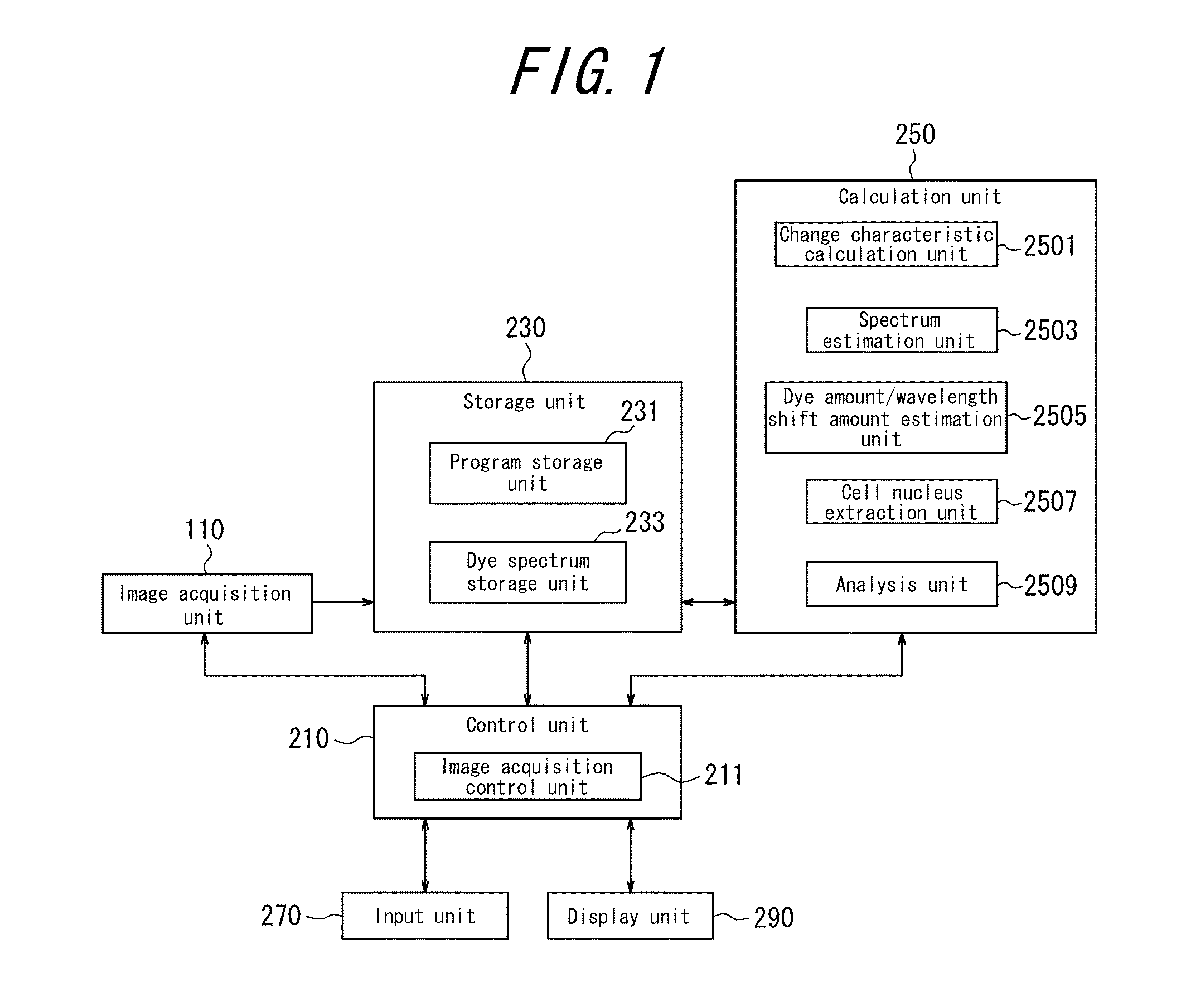
[0076]FIG. 1 is a block diagram illustrating the functional structure of main portions of an image processing device according to Embodiment 1 of the present invention. This image processing device is formed by a microscope and a computer, such as a personal computer, and includes an image acquisition unit 110, an input unit 270, a display unit 290, a calculation unit 250, a storage unit 230, and a control unit 210 that controls each of the other units.

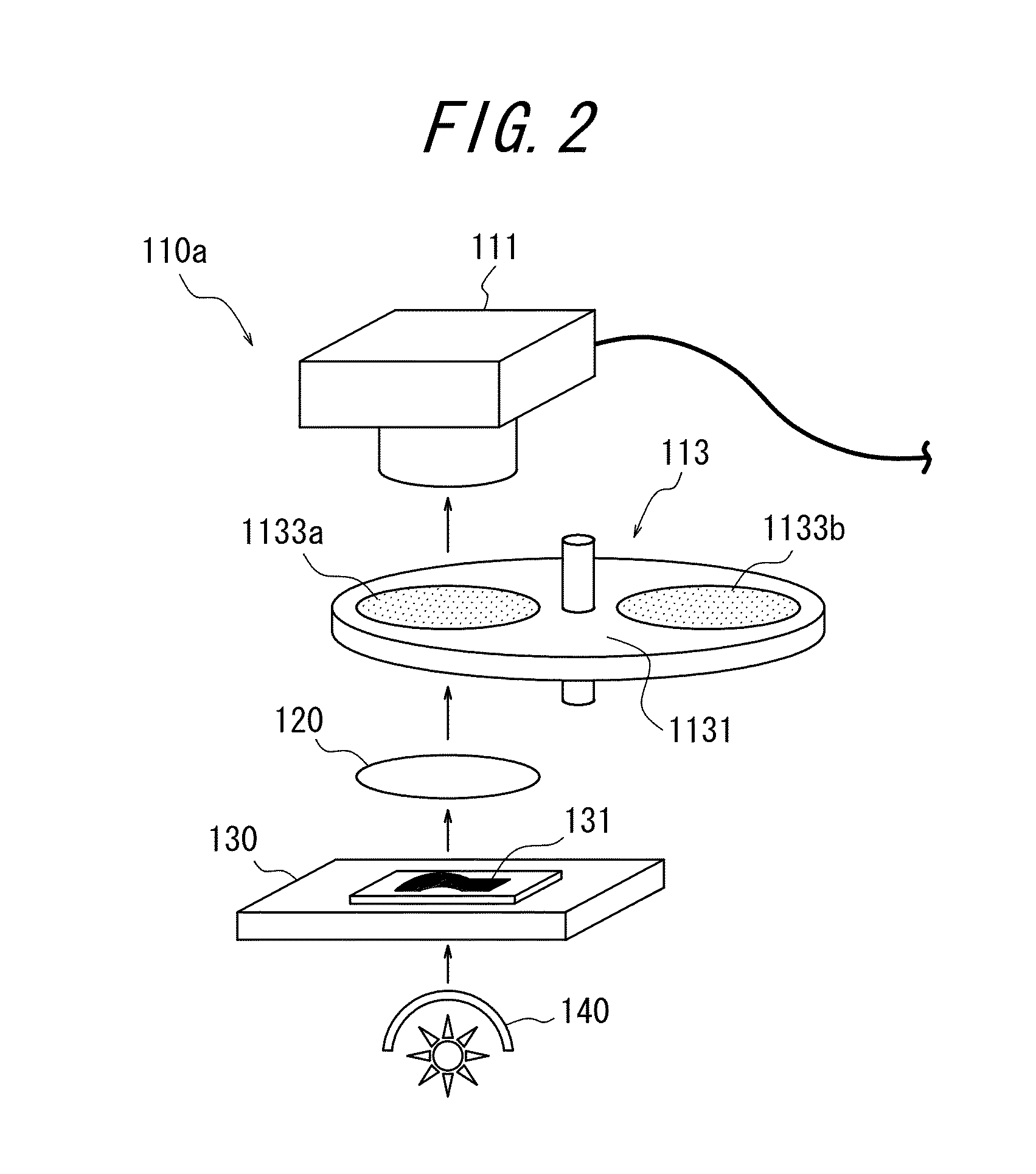
[0077]The image acquisition unit 110 acquires a multiband image (in the present embodiment, a six-band image), and for example as illustrated in FIG. 2, includes an RGB camera 111 and a filter unit 113 for restricting the wavelength band of light that forms an image on the RGB camera 111 to be in a predetermined range.

[0078]The RGB camera 111 includes an imaging element such as a Charge Coupled Device (CCD), a Complementary Metal Oxide Semiconductor (CMOS), or the like and for example has the spectral sensitivity characteristics of th...

embodiment 2

[0103]FIG. 11 is a block diagram illustrating the functional structure of main portions of an image processing device according to Embodiment 2 of the present invention. In the context of the structure of Embodiment 1, this image processing device corrects the dye amount based on the information on the cell nucleus region and displays the target sample image on the display unit 290 based on the corrected dye amount. Accordingly, instead of the analysis unit 2509 in FIG. 1, the calculation unit 250 includes a dye amount correction coefficient calculation unit 2509a, a dye amount correction unit 2511, and a display image creation unit 2513. The storage unit 230 is provided with a dye amount standard value storage unit 235 that stores a dye amount standard value dstd(i) for the cell nucleus region. The remaining structure is similar to Embodiment 1, and therefore a description thereof is omitted.

[0104]FIG. 12 is a flowchart providing an overview of operations by the image processing de...

embodiment 3

[0112]FIG. 13 is a block diagram illustrating the functional structure of main portions of a virtual microscope system according to Embodiment 3 of the present invention. The virtual microscope system acquires a virtual slide image of a stained sample and includes a microscope device 400 and a host system 600.

[0113]The microscope device 400 includes a microscope body 440 having a reversed square C shape when viewed from the side, a light source 480 attached at the back side of the bottom of the microscope body 440, and a lens tube 490 placed on the top of the microscope body 440. The microscope body 440 supports a motor-operated stage 410 on which a target sample S is placed and holds an objective lens 470 via a revolver 460. A binocular unit 510 for visual observation of a sample image of the target sample S and a TV camera 520 for capturing the sample image of the target sample S are attached to the lens tube 490. In other words, the microscope device 400 corresponds to the image ...


PUM


Abstract

An image processing device for processing a stained sample image including hematoxylin stain is provided with a dye spectrum storage unit that stores a dye spectrum of dye used in staining, a change characteristic calculation unit that calculates a change characteristic in a wavelength direction of the dye spectrum based on the dye spectrum, a dye amount/wavelength shift amount estimation unit that estimates at least a dye amount of the hematoxylin stain and a shift amount in the wavelength direction for each pixel in the stained sample image based on the dye spectrum and the change characteristic; and a cell nucleus extraction unit that extracts a cell nucleus region of the stained sample image based on the shift amount estimated in the wavelength direction.

Description

CROSS REFERENCE TO RELATED APPLICATION[0001]The present application is a Continuing Application based on International Application PCT / JP2012 / 059423 filed on Mar. 30, 2012, which, in turn, claims the priority from Japanese Patent Application No. 2011-102477 filed on Apr. 28, 2011, the entire disclosure of these earlier applications being herein incorporated by reference.TECHNICAL FIELD[0002]The present invention relates to an image processing device, an image processing method, an image processing program, and a virtual microscope system.BACKGROUND ART[0003]A spectral transmittance spectrum is one physical quantity representing a physical property specific to an object. The spectral transmittance is a physical quantity representing a ratio of transmitted light to incident light at each wavelength and is specific to an object, having a value that does not change due to extrinsic influences, unlike color information such as an RGB value that varies depending on changes in illumination...

Claims


Application Information

Patent Timeline
Patent Type & Authority Applications(United States)
IPC IPC(8): G06T7/00
CPCG06T7/0012G06T2207/10056G06T2207/30024G06T7/11G06V20/695
Inventor OTSUKA, TAKESHI
Owner OLYMPUS CORP
Why Eureka
Try Eureka