Semiconductor module cooler and semiconductor module

Active Publication Date: 2014-02-13
FUJI ELECTRIC CO LTD
View PDF3 Cites 37 Cited by
  • Summary
  • Abstract
  • Description
  • Claims
  • Application Information

AI Technical Summary

Benefits of technology

[0022]With the semiconductor module cooler according to the present invention, by setting a cross-sectional area of an introduction channel smaller than that of a discharge channel so that the coolant flows toward one of the side surfaces of a heat sink, a flow velocity of the coolant in the vicinity of the inlet can be increased to resolve increased temperature of the vicinity of the inlet and a flow velocity of the coolant which flows into the heat sink from the first flow channel can be adjusted.
[0023]In addition

Problems solved by technology

Therefore, with a semiconductor module comprising a plurality of power semiconductor devices, the methods of cooling the power semiconductor devices pose a major problem.
However, increasing a coolant flow rate to the cooling apparatus or adopting a fin shape with a high heat transfer rate is likely to cause inconveniences such as increased pressure loss of a coolant flowing inside the apparatus.
In particular, with a cooling apparatus that cools a large number of power semiconductor devices using a plurality of heat sinks, when using a serpentine flow channel which connects a plurality of flow channels in series, there is a significant increase in pressure loss.
While this can be achieved by, for example, increasing thermal conductivity of the fin material, adopting a new fin material may result in increasing overal

Method used


Image

  • Semiconductor module cooler and semiconductor module
  • Semiconductor module cooler and semiconductor module
  • Semiconductor module cooler and semiconductor module

Examples


first embodiment

[0100]In the first embodiment, a cooler 2 in which a width of the coolant introduction flow channel 21 has been reduced in order to adjust a disproportionate flow in the semiconductor module will be described.

[0101]FIGS. 9(A), 9(B) are plan views showing a guide section shape of a water jacket used in the semiconductor module according to the present invention. In the two water jackets 2A shown in FIGS. 9(A) and 9(B), the inlet 24 and the outlet 25 are arranged on the left sidewall 2Ab thereof in a similar manner to the conventional type A shown in FIG. 6(B). However, the inlet section 21a which guides the coolant from the inlet 24 to the coolant introduction flow channel 21 and the outlet section 22a for effusing the coolant from the coolant discharge flow channel 22 to the outlet 25 are formed longer than those shown in FIG. 6(B) and FIG. 3. In other words, the inlet section 21a and the outlet section 22a are formed so as to protrude from the same left sidewall 2Ab.

[0102]In a type...

second embodiment

[0128]In the second embodiment, a cooler will be described in which the flow channel width of the coolant introduction flow channel 21 is formed narrow as in the first embodiment by providing a separation wall in the coolant introduction flow channel 21 and dividing the flow channel of the coolant into a plurality of flow channels.

[0129]FIGS. 14(A), 14(B) are diagrams showing a water jacket used in the semiconductor module according to the present invention, wherein FIG. 14(A) is a plan view showing a guide section shape of a water jacket and FIG. 14(B) is a perspective view showing the water jacket in FIG. 14(A).

[0130]In the type H water jacket 2A shown in FIG. 14(A), the inlet section 21a and the outlet section 22a are respectively set to an equal flow channel width w1 (for example, 15 mm) on the side of the inlet 24 and on the side of the outlet 25. The inlet section 21a which guides the coolant from the inlet 24 to the coolant introduction flow channel 21 and the outlet section ...

third embodiment

[0151]Next, a water jacket 2A provided with the separation wall that is not inclined will be described as the third embodiment.

[0152]In the second embodiment, since the guide section 21Si provided on the side of the inner surface of the front sidewall 2Aa facing the fins 2C of the water jacket 2A has a predetermined angle of inclination, the separation wall 27 which divides the flow channel of the coolant is also provided with an angle of inclination toward the side of the fins 2C in a downstream direction. However, from the perspective of ease of water jacket manufacturing technology, desirably, the separation wall 27 is arranged parallel to the front sidewall 2Aa and improves cooling performance at the trailing end position B7 of the coolant introduction flow channel 21.

[0153]FIGS. 19(A), 19(B) are diagrams showing a water jacket used in the semiconductor module according to the present invention, wherein FIG. 19(A) is a plan view showing a guide section shape of a water jacket an...


PUM


Abstract

A semiconductor module cooler supplies a coolant to a water jacket from outside and cools a semiconductor device arranged on an outer surface of the cooler. The semiconductor module cooler has a heat sink thermally connected to the semiconductor device; a first flow channel arranged inside the water jacket with a guide section extending from a coolant inlet and having an inclined surface for guiding the coolant toward one side surface of the heat sink; a second flow channel arranged inside the water jacket in parallel to the first flow channel and extending to a coolant outlet; and a third flow channel formed inside the water jacket at a position connecting the first flow channel and the second flow channel. The coolant inlet and the coolant outlet are formed on a same wall surface of the water jacket, and the heat sink is arranged in the third flow channel.

Description

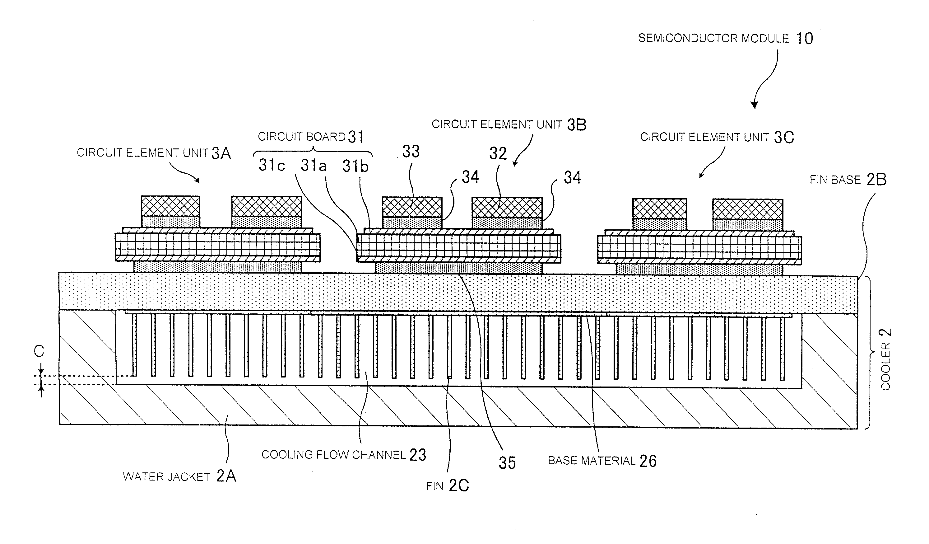
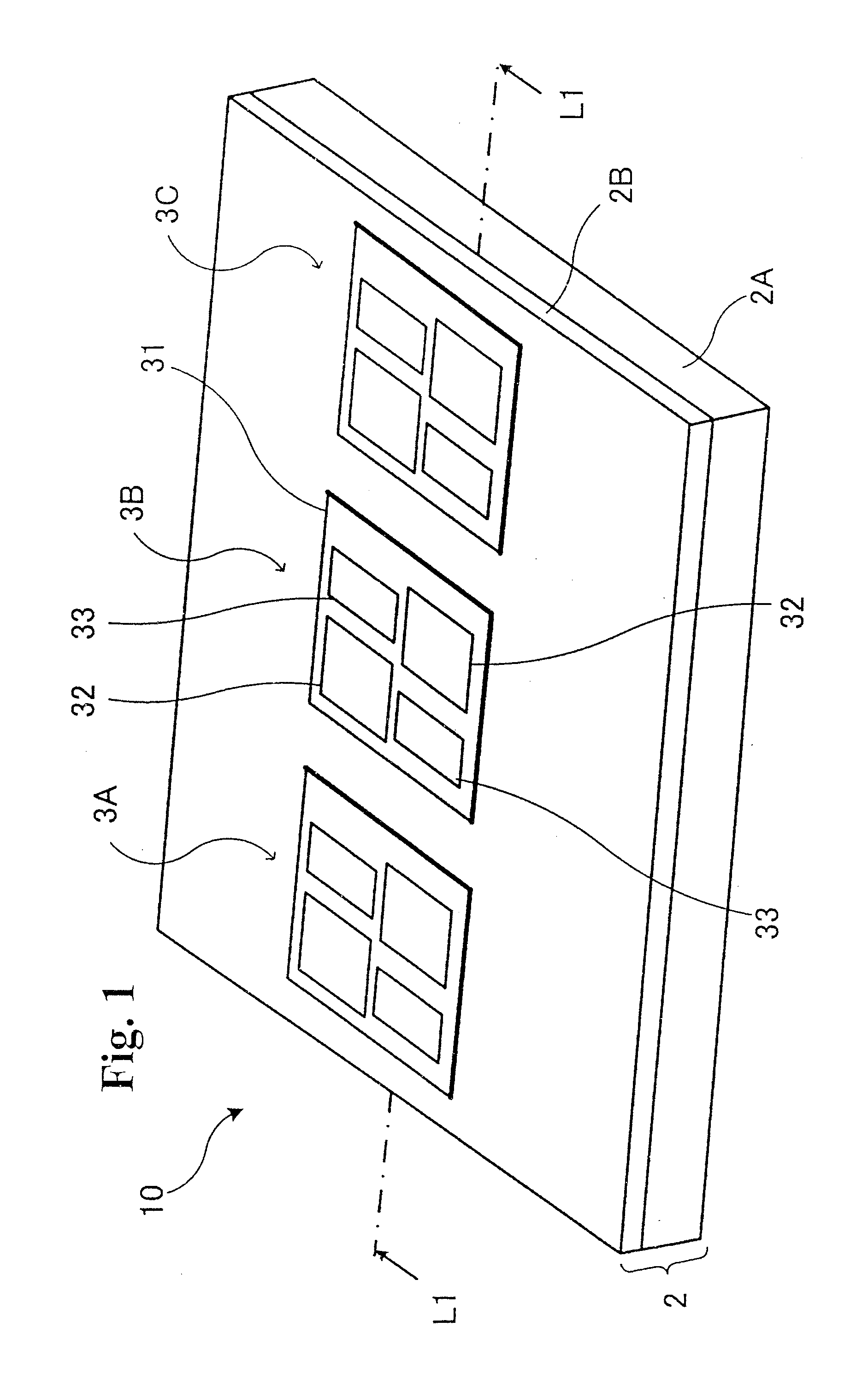
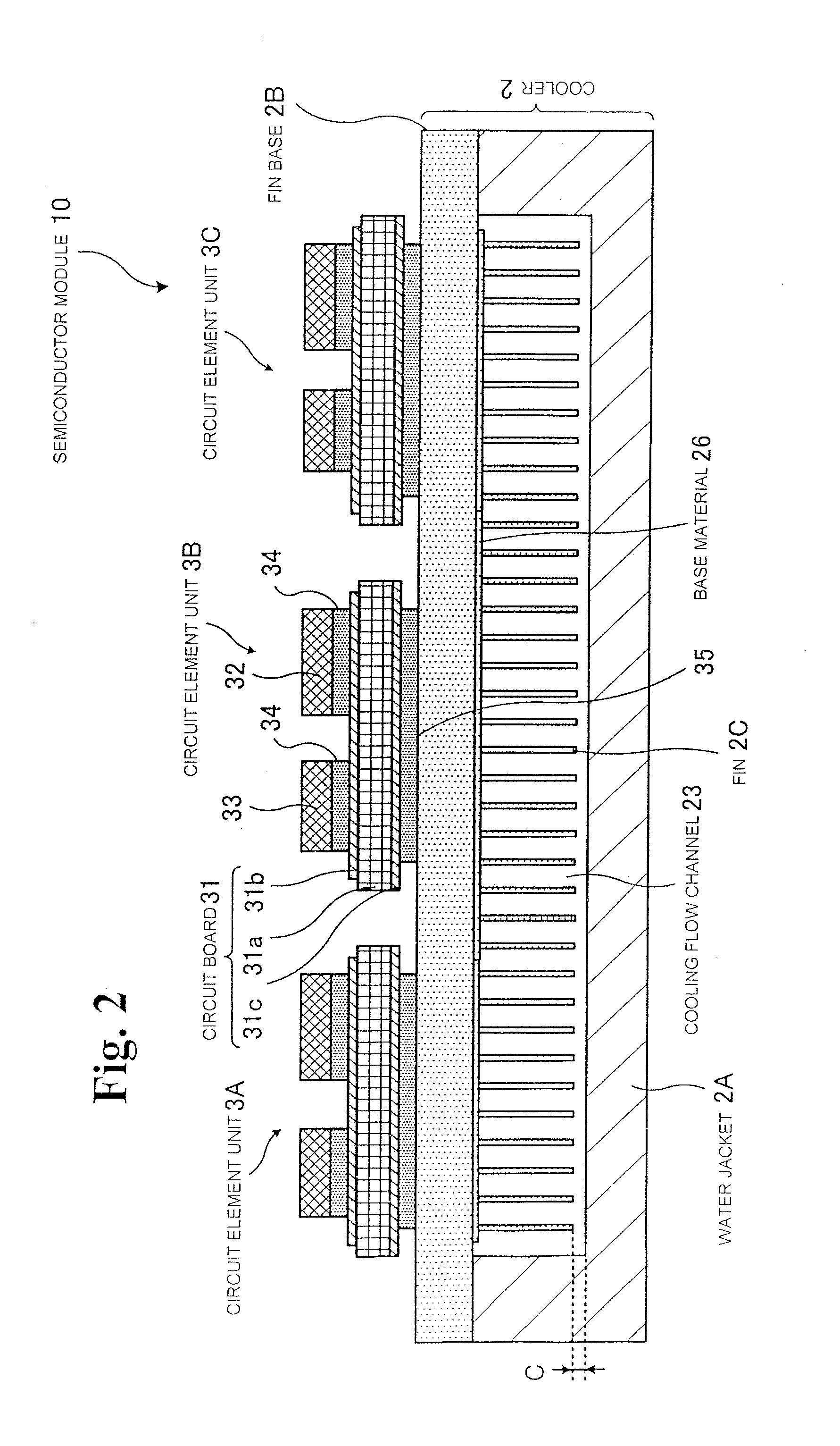
TECHNICAL FIELD[0001]The present invention relates to a semiconductor module cooler which supplies a coolant to a water jacket from outside to cool a semiconductor device arranged on an outer surface of the cooler and to a semiconductor module provided with the semiconductor module cooler.BACKGROUND ART[0002]For power converters represented in hybrid cars, electric vehicles, and the like, semiconductor modules are widely used. Semiconductor modules that constitute a controller for energy conservation comprise power semiconductor devices in order to control large currents.[0003]Such power semiconductor devices are generating more and more heat when controlling large currents. In particular, the amount of heat generation increases significantly as the sizes of power semiconductor devices are reduced and output of power semiconductor devices is increased. Therefore, with a semiconductor module comprising a plurality of power semiconductor devices, the methods of cooling the power semic...

Claims


Application Information

Patent Timeline
IPC IPC(8): H05K7/20
CPCH05K7/20254H01L23/3735H01L23/473H05K7/20927H01L2224/32225H01L2924/13055H01L2924/1305H01L2924/00
Inventor GOHARA, HIROMICHIMOROZUMI, AKIRAICHIMURA, TAKESHI
Owner FUJI ELECTRIC CO LTD
Why Eureka
Try Eureka