

Semiconductor device
- Summary
- Abstract
- Description
- Claims
- Application Information
AI Technical Summary
Benefits of technology
Problems solved by technology
Method used
Image

Examples
first embodiment
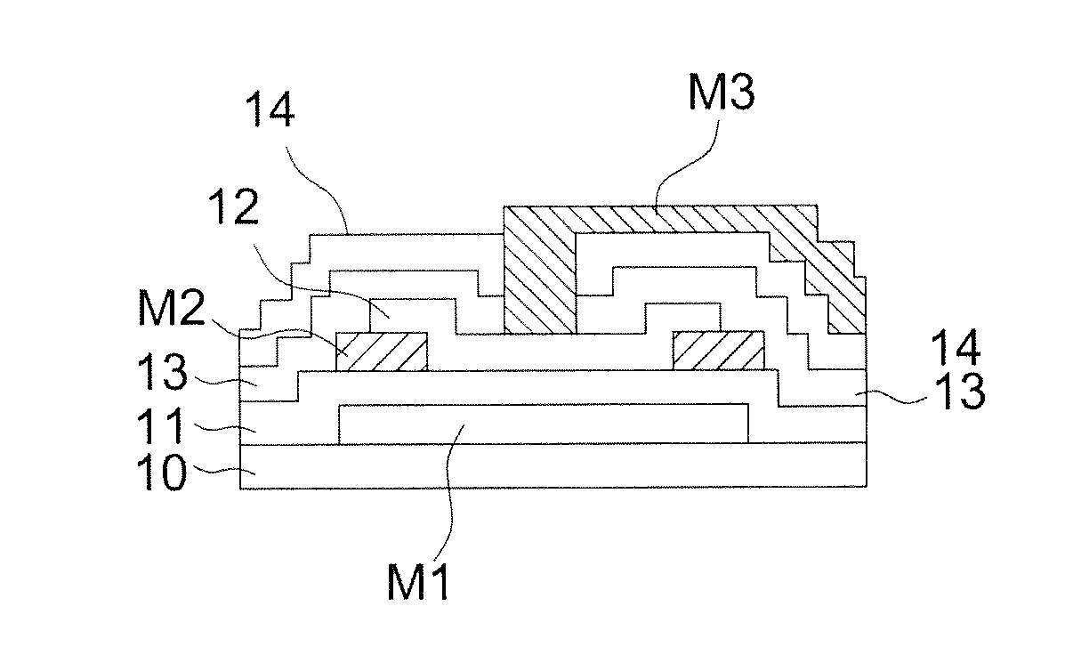
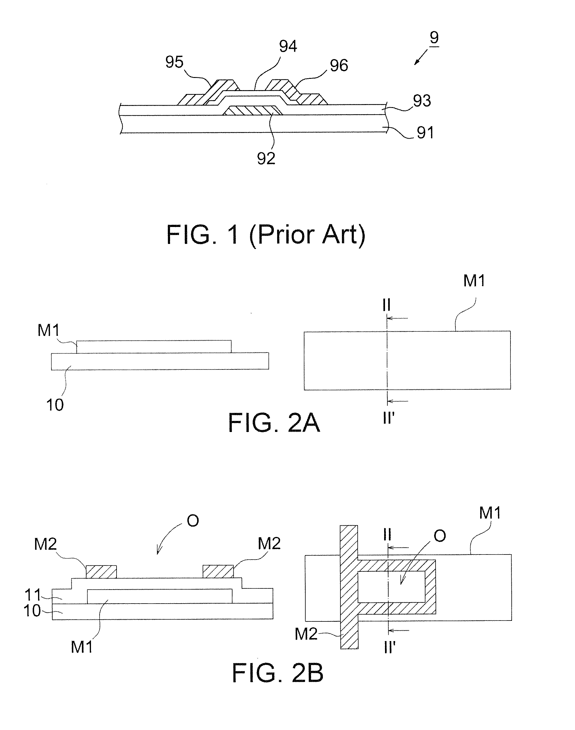
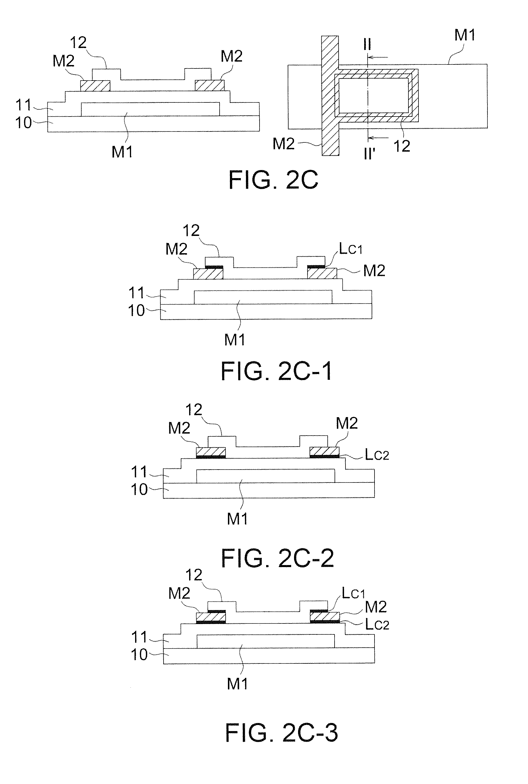
[0030]Referring to FIGS. 2A-2E, they show manufacturing processes of the semiconductor device according to the present disclosure. In FIGS. 2A-2C and 2D-2E, the right part is a top view of the semiconductor device and the left part is a cross-sectional view take along line II-II′ in the top view. It should be mentioned that, for simplification, the top views in FIGS. 2A-2E only show the conductive layers M1-M3 and the channel layer 12 without showing the substrate 10, the insulating layer 11, the passivation layer 13 and contact layers LC1, LC2, wherein the top views are mainly to show the arrangement of the conductive layers M1-M3. In the present disclosure, the semiconductor device may be a thin film transistor (TFT) device.
[0031]Firstly, a substrate 10 is provided. The substrate 10 may be a glass substrate or other substrates adapted to form a thin film transistor array thereon.
[0032]As shown in FIG. 2A, a first conductive layer M1 is then formed on the substrate 10 to be served ...
second embodiment
[0044]Referring to FIGS. 4A and 4B, they show manufacturing processes of the semiconductor device according to the present disclosure, wherein methods of forming the first conductive layer M1, the insulating layer 11, the second conductive layer M2, the channel layer 12 and the passivation layer 13 are similar to FIGS. 2A-2D and their corresponding descriptions, and thus details thereof are not repeated herein. Similarly, for simplification, the top view (i.e. the right part) of FIGS. 4A-4B only shows the conductive layers M1-M3, the channel layer 12 and the transparent electrode layer 15 without showing the substrate 10, the insulating layer 11 and the passivation layer 13. The left part is also the cross-sectional view taken along line II-II′ of the right part.
[0045]Referring to FIG. 4A, in the second embodiment, in order to increase the contact feature between the channel layer 12 and the transparent electrode layer, a third conductive layer M3 is previously formed in the contact...
PUM
 Abstract
Description
Claims
Application Information