WDM telecommunications link with coherent detection and optical frequency comb sources

a technology of optical frequency comb and telecommunications link, which is applied in the field of optical link combining, can solve the problems of phase and frequency lock, difficulty in realization, and mode locking of comb components, and achieve the effect of facilitating the demodulation of a large number of coherently detected optical channels and reducing the frequency of residual intermediate frequencies

Active Publication Date: 2014-03-06
RWTH AACHEN UNIV
View PDF0 Cites 49 Cited by
  • Summary
  • Abstract
  • Description
  • Claims
  • Application Information

AI Technical Summary

Benefits of technology

[0022]The present invention relates to an optical link combining wavelength domain multiplexing (WDM) with coherent detection. The receiver light source for more than one WDM channel is implemented in the form of an optical frequency comb source. The transmitter light source for said more than one WDM channels is implemented in the form of another frequency comb source. Constant or approximately constant frequency offsets and / or phase offsets between the frequency components of the optical combs are used to reduce the number of optical phase locked loops (OPLL), electrical phase locked loops (EPLL) or feed-forward carrier recovery in the system. A combination of two of one of an OPLL, an EPLL or a feed-forward carrier recovery is utilized to completely lock a mode-locked receiver frequency comb source to a mode-locked transmitter frequency comb source. In the absence of good frequency comb mode-locking, approximately constant frequency offsets of the optical combs can still be used to replace all but one of the PLLs by slow digital phase locked loops or slow digital feed-forward carrier recovery. The method is suitable to a large number of channels.
[0023]More specifically, the present invention relates to a WDM link implementing coherent detection at a receiver where a mode locked optical frequency comb source is utilized as a multi-carrier-frequency light source at a transmitter and a mode locked optical frequency comb source is utilized as a multi-frequency-component local light source at said receiver. The multi-frequency-component local light source provides the individual frequency components required to coherently detect incoming optical channels. Coherent detection and demodulation is implemented with a reduced number of phase locked loops or feed forward carrier recovery systems. The architecture leverages the mode locked nature of the transmitter and receiver light sources in order to achieve this reduction in complexity. The reduced complexity can result in more compact systems, cheaper systems or systems with lower power consumption. The local multi-frequency-component light source of the receiver is called the receiver optical comb source and generates the receiver optical comb. The multi-carrier-frequency light source at the transmitter is called the transmitter optical comb source and generates the transmitter optical comb. In the context of OPLLs, one comb source is at least partially controlled according to another comb source. The controlled comb source is then called the slave comb source and the other comb source is then called the master comb source. The slave comb source is typically the receiver comb source and the master comb source is typically the transmitter comb source, but this is not necessarily the case as other architectures are also described. In an OPLL, an optical oscillator, here in the form of an optical comb source, is controlled with a control signal. This control signal allows adjusting the center frequencies of individual comb components, the frequency offset between adjacent frequency comb components, or a combination thereof. Two control signals are said to allow independent control of center frequency and of frequency offset if center frequency and frequency offset can be independently adjusted by a combination of the two control signals. This is mathematically defined in a later paragraph. Two optical PLLs are said to be independent of each other if they adjust control signals that allow independent control of center frequency and frequency offsets.
[0024]In a mode locked optical frequency source, both the frequency offset and the phase offset between adjacent frequency components have a fixed value independent on which two adjacent frequency components are considered. This frequency and phase locking inherent to the optical frequency comb source allows a drastic reduction of system complexity. Indeed, there are only 4 degrees of freedom describing an ideal mode locked frequency comb, the angular frequency ω0 and phase φ0 of one of the comb components, hereafter called the component of index 0, and the angular frequency difference Δω and phase difference Δφ between adjacent frequency components. The frequency difference Δω is called the free spectral range (FSR) of the optical comb. The frequency components of the optical comb are numbered with an index, with smaller index for components at lower frequencies and higher index for components at higher frequencies. In the following descriptions, when two frequency combs that are at least roughly aligned are described in the context of the coherent detection WDM system, frequency components of the two combs that fall within the same WDM frequency window, as defined by the implemented frequency domain demultiplexer(s) in the receiver, are attributed the same index.

Problems solved by technology

In other cases nonlinear processes inside the laser such as four wave mixing can lead to mode locking of the comb components.
One difficulty with homodyne coherent detection is to phase and frequency lock the local light source with the center frequency and average phase of the incoming optical channel.
PLLs are very sensitive to delays in the feedback path making their realization challenging.
The data can also be directly demodulated in the digital domain, in this case however one difficulty resides in the fact that the signals have to be typically sampled at the Nyquist rate and very high speed ADCs are required.
This results in a high system complexity and a high number of costly components.
One of the drawbacks of Silicon Photonics is that it is a technology with high optical losses at fiber to chip interfaces and within optical modulators.
Silicon photonics is also a technology that allows easily duplicating devices in a single chip, thus increasing system complexity at little additional cost and space.

Method used


Image

  • WDM telecommunications link with coherent detection and optical frequency comb sources
  • WDM telecommunications link with coherent detection and optical frequency comb sources
  • WDM telecommunications link with coherent detection and optical frequency comb sources

Examples


Embodiment Construction

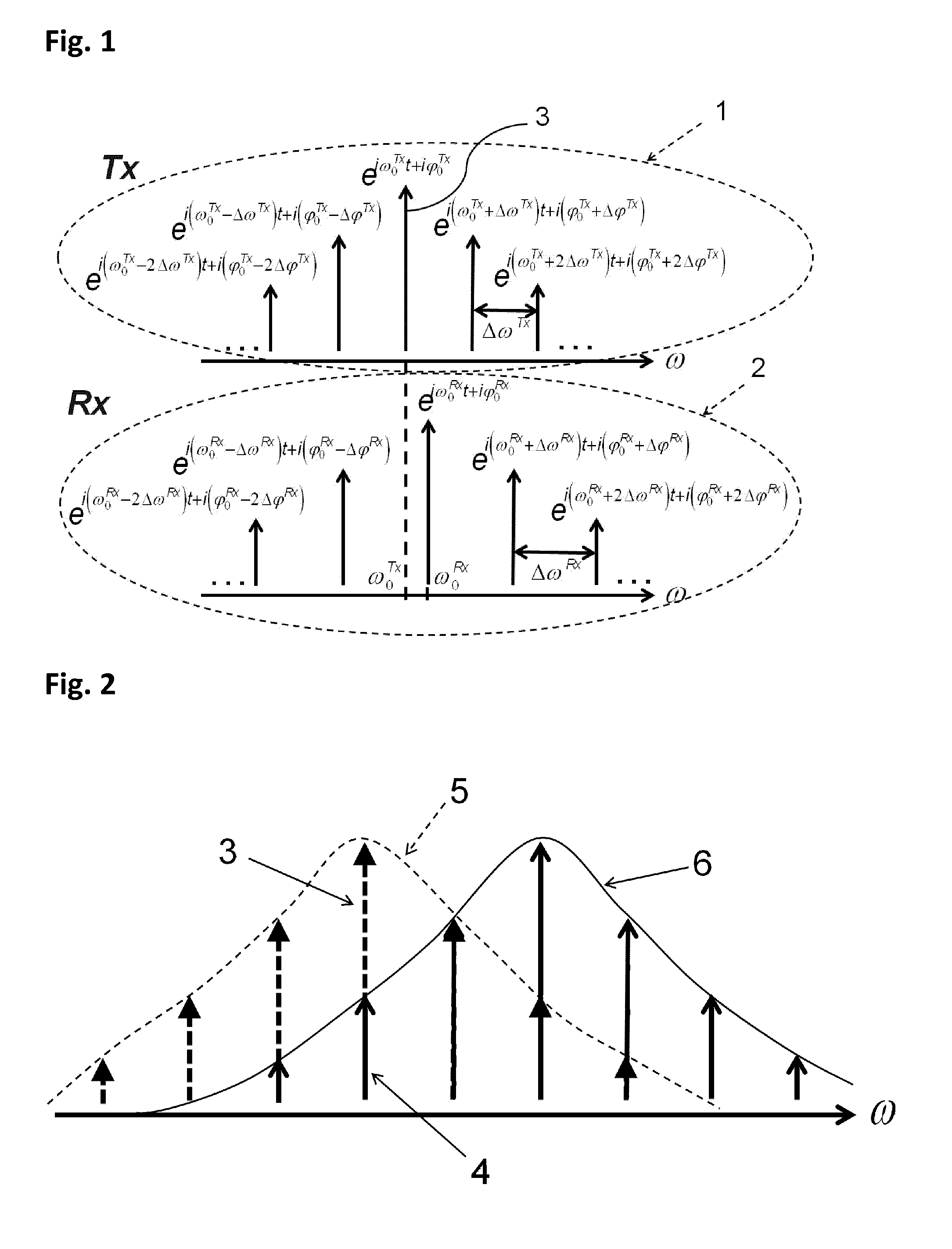
[0078]In FIG. 1, a transmitter Tx mode-locked frequency comb spectrum 1 and a receiver Rx mode-locked frequency comb spectrum 2 are shown. A frequency comb component 3 of the transmitter Tx frequency comb has a frequency ω0Tx and a phase φ0Tx. The transmitter Tx comb has a free spectral range (also called frequency offset of the transmitter comb) ΔωTx and a phase offset ΔφTx. Similar notation hold for the receiver Rx comb. The vertical axis represents the power level of the frequency comb components. The difference between the frequencies of the frequency comb components of index 0 of the two combs is illustrated.

[0079]In FIG. 2 the frequency comb components 3 of the transmitter Tx comb are represented with one type of arrow (dashed, filled arrow tip) and, frequency components 4 of the receiver Rx comb are represented with another type of arrow (continuous). As shown, the two combs are locked to each other, but the envelope functions 5 and 6 of the transmitter Tx and receiver Rx com...


PUM


Abstract

An optical data link has a transmitter and a receiver with coherent detection at the receiver and more than one optical carrier frequency. The optical carrier frequencies are generated by a frequency comb source in both the transmitter and the receiver. The frequency comb sources generate frequency combs that have frequency components and a free spectral range. The optical carrier frequencies transport more than one optical channel. Either at least one frequency component or the free spectral range of the optical comb generated at the receiver is locked to the comb generated at the transmitter by an optical phase locked loop, or an electrical phase locked loop or a feed-forward carrier recovery generates an intermediate frequency carrier reference that is routed to more than one channel to demodulate the data.

Description

CROSS-REFERENCE TO RELATED APPLICATIONS[0001]This application is the U.S. National Phase of International Application No. PCT / EP2012 / 057829, filed Apr. 27, 2012, claiming benefit of U.S. Provisional Patent Application No. 61 / 481,159, filed Apr. 30, 2011, the contents of which are hereby incorporated by reference in their entirety as part of the present disclosure.FIELD OF THE INVENTION[0002]The present invention relates to an optical link combining wavelength domain multiplexing (WDM) with coherent detection.BACKGROUND OF THE INVENTION[0003]An optical frequency comb is light with an optical spectrum consisting of multiple discrete frequency components. The frequency difference between adjacent frequency components is substantially constant and called the frequency offset. The phase difference between adjacent frequency components is substantially constant and called the phase offset. In other words, individual frequency components are described by exp(i×ωjt+φj) where i is the index ...

Claims


Application Information

Patent Timeline
Patent Type & Authority Applications(United States)
IPC IPC(8): H04B10/61H04J14/02
CPCH04J14/02H04B10/6164H04B10/64H04J14/002
Inventor WITZENS, JEREMY
Owner RWTH AACHEN UNIV
Why Eureka
Try Eureka