Semiconductor device and semiconductor device manufacturing method

a semiconductor device and semiconductor technology, applied in the direction of semiconductor devices, basic electric elements, electrical appliances, etc., can solve the problems of thermal runaway destruction, high production cost, and high production cost, and achieve the effect of suppressing the implantation of holes, reducing the occurrence of leakage current, and gentle concentration gradien

Active Publication Date: 2014-03-13
FUJI ELECTRIC CO LTD
View PDF1 Cites 30 Cited by
  • Summary
  • Abstract
  • Description
  • Claims
  • Application Information

AI Technical Summary

Benefits of technology

[0024]According to the invention, the amount of holes implanted from the collector side when a short circuit occurs increases, and the rise of a magnetic field intensity on the collector side is suppressed, by forming a first conductivity type field-stop layer that is deep and of a low impurity concentration, and that has a gentle concentration gradient, using selenium or sulfur as a dopant. Also, by providing a first conductivity type buffer layer having a predetermined peak impurity concentration between the first conductivity type field-stop layer and a second conductivity type collector layer using an ion implantation of phosphorus, it is possible to suppress an implantation of holes contributing to an increase in leakage current. Also, according to the invention, it is possible to reduce on-sta...

Problems solved by technology

However, a thin wafer is liable to crack during the manufacturing process, causing the efficiency rate to deteriorate, because of which a wafer that has not been thinned is used as it is when being introduced into the manufacturing process.
The hole injection efficiency bein...

Method used


Image

  • Semiconductor device and semiconductor device manufacturing method
  • Semiconductor device and semiconductor device manufacturing method
  • Semiconductor device and semiconductor device manufacturing method

Examples


embodiment

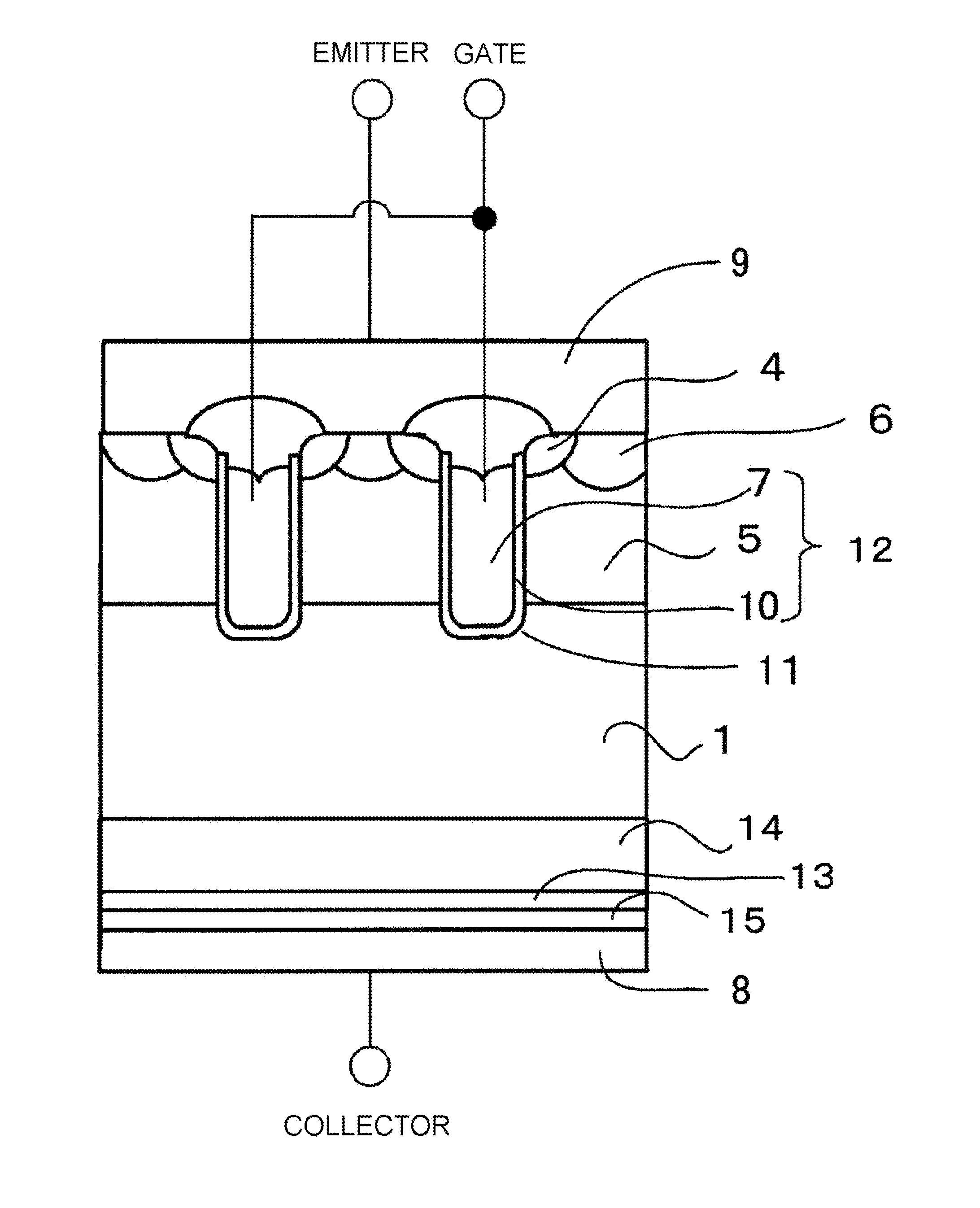
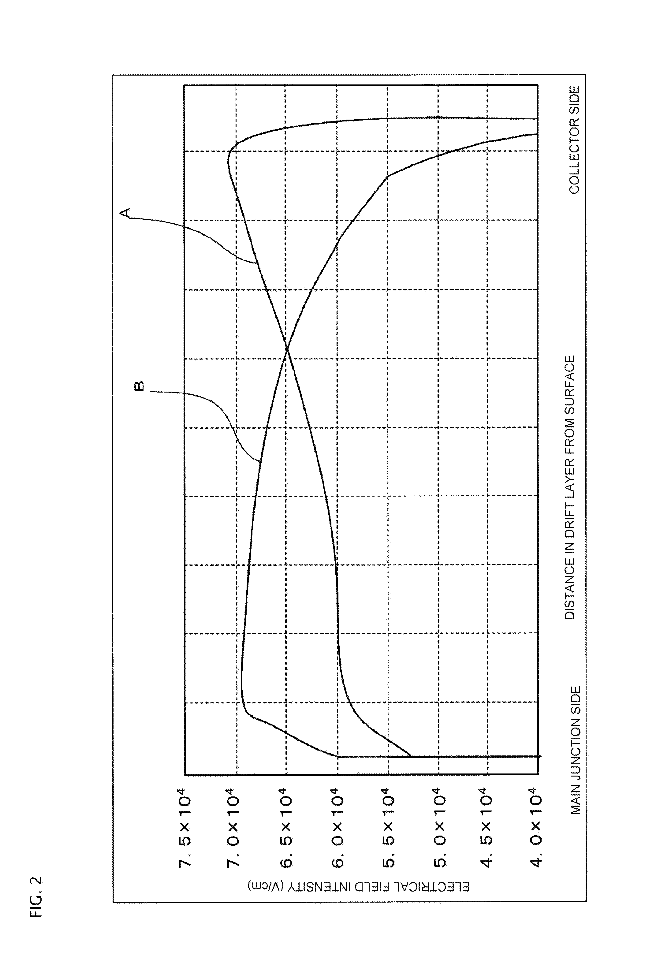
[0034]A field-stop IGBT (FS-IGBT) according to an embodiment of the invention will be described in detail with reference to FIGS. 1, 6 and the like, with a trench-FS-IGBT with a breakdown voltage of, for example, 1,700V as an example. FIG. 1 is a main portion sectional view showing the configuration of the FS-IGBT according to the embodiment of the invention. FIG. 6 is a characteristic diagram showing the impurity concentration distribution of the FS-IGBT according to the embodiment of the invention. FIG. 6 shows the impurity concentration distribution from the back surface to an n− type drift layer 1 of a silicon (Si) substrate (semiconductor substrate) configuring the trench-FS-IGBT (the same also applies to FIG. 7).

[0035]The trench-FS-IGBT shown in FIG. 1 is configured using, for example, an FZ-n-type Si substrate formed of an inexpensive FZ wafer. The resistivity of the Si substrate may be in the region of, for example, 80 Ωcm to 130 Ωcm. The thickness of the finished Si substra...


PUM


Abstract

In some aspects of the invention, an n-type field-stop layer can have a total impurity of such an extent that a depletion layer spreading in response to an application of a rated voltage stops inside the n-type field-stop layer together with the total impurity of an n type drift layer. Also, the n-type field-stop layer can have a concentration gradient such that the impurity concentration of the n-type field-stop layer decreases from a p+ type collector layer toward a p-type base layer, and the diffusion depth is 20 μm or more. Furthermore, an n+ type buffer layer of which the peak impurity concentration can be higher than that of the n-type field-stop layer at 6×1015 cm−3 or more, and one-tenth or less of the peak impurity concentration of the p+ type collector layer, can be included between the n-type field-stop layer and p+ type collector layer.

Description

[0001]This application is a continuation of International Application No. PCT / JP2012 / 062875, filed on May 18, 2012, which is based on and claims priority to Japanese Patent Application No. JP PA 2011-111709, filed on May 18, 2011. The disclosure of the Japanese priority application and the PCT application in their entirety, including the drawings, claims, and the specification thereof, are incorporated herein by reference.BACKGROUND[0002]1. Field of the Invention[0003]Embodiments of the invention relate to a semiconductor device and semiconductor device manufacturing method, and in particular, relate to a semiconductor device and semiconductor device manufacturing method such that a field-stop layer is provided on a substrate back surface side.[0004]2. Related Art[0005]An IGBT (Insulated Gate Bipolar Transistor) is a power element wherein the high speed switching characteristics and voltage drive characteristics of a MOSFET (Metal-Oxide-Semiconductor Field Effect Transistor) and the...

Claims


Application Information

Patent Timeline
IPC IPC(8): H01L29/739
CPCH01L29/7395H01L21/26513H01L21/2855H01L21/324H01L29/0615H01L29/0619H01L29/0804H01L29/0821H01L29/0834H01L29/0847H01L29/1004H01L29/1095H01L29/167H01L29/36H01L29/4236H01L29/66348H01L29/7397
Inventor YOSHIMURA, TAKASHIKURIBAYASHI, HIDENAOONOZAWA, YUICHINAKANO, HAYATOOZAKI, DAISUKE
Owner FUJI ELECTRIC CO LTD
Why Eureka
Try Eureka