Fabricating a semiconductor die having coefficient of thermal expansion graded layer

Inactive Publication Date: 2014-03-20
TEXAS INSTR INC
View PDF0 Cites 1 Cited by
  • Summary
  • Abstract
  • Description
  • Claims
  • Application Information

AI Technical Summary

Benefits of technology

This patent describes a semiconductor device that includes a substrate with circuit elements such as transistors and capacitors. The device also includes a multi-layer structure made of different materials with a varying coefficient of thermal expansion (CTE). A CTE graded layer is used to provide a graded CTE that increases from one side to the other, which can help achieve better performance and reliability of the device. The multi-layer structure can also include through-substrate-vias (TSVs) that extend through the full thickness of the substrate. The patent also mentions the use of a "metal layer" and a "multi-phase material" which has a single chemical composition but is made up of different materials that differ in chemical composition.

Problems solved by technology

In the case of highly mobile metal TSV filler materials that are known to significantly reduce minority carrier lifetimes in the semiconductor, such as copper in the case of silicon, migration can cause problems such as significantly increased junction leakage or a shift in transistor threshold voltage.
For example, around room temperature copper has a CTE of approximately 17 ppm / ° C., whereas silicon has a CTE of approximately 2 to 3 ppm / ° C., while silicon dioxide has a CTE of about 0.6 ppm / ° C. Such CTE mismatches (ΔCTE) can result in significant thermally induced stress in the TSV as well as the silicon substrate including the circuitry (e.g. MOS transistors) in the silicon (or bother substrate material) surrounding the TSVs, particularly during certain fab processing subsequent to the fabrication of the TSV (e.g., 360° C. to 410° C. sinters), during assembly and test / operations as may occur during solder reflow (e.g., up to about 260° C.) or during thermo-compressive bonding (e.g., up to 400° C.
he CTE mismatch between the dielectric liner and TSV filler material can lead to diffusion barrier metal layer failures (e.g., ruptures or peeling) which allows metal (e.g., copper) migration into the substrate.

Method used


Image

  • Fabricating a semiconductor die having coefficient of thermal expansion graded layer
  • Fabricating a semiconductor die having coefficient of thermal expansion graded layer
  • Fabricating a semiconductor die having coefficient of thermal expansion graded layer

Examples


Embodiment Construction

[0015]Example embodiments are described with reference to the drawings, wherein like reference numerals are used to designate similar or equivalent elements. Illustrated ordering of acts or events should not be considered as limiting, as some acts or events may occur in different order and / or concurrently with other acts or events. Furthermore, some illustrated acts or events may not be required to implement a methodology in accordance with this disclosure.

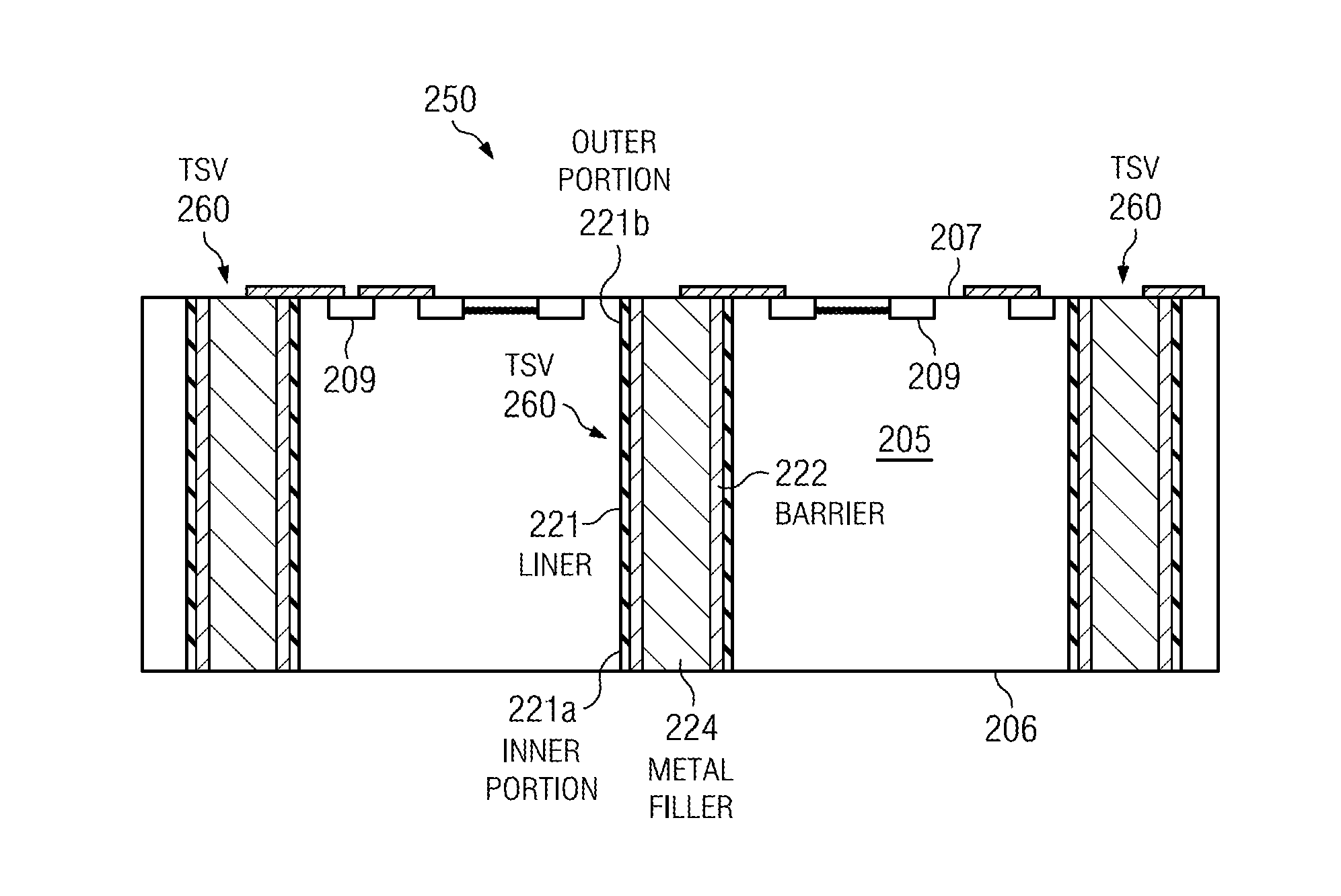
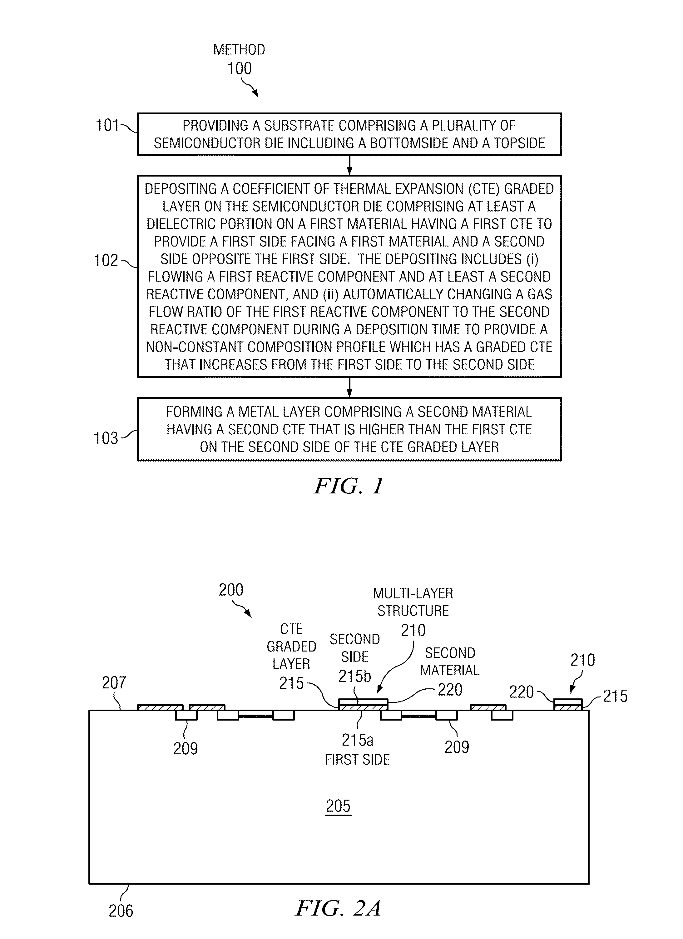
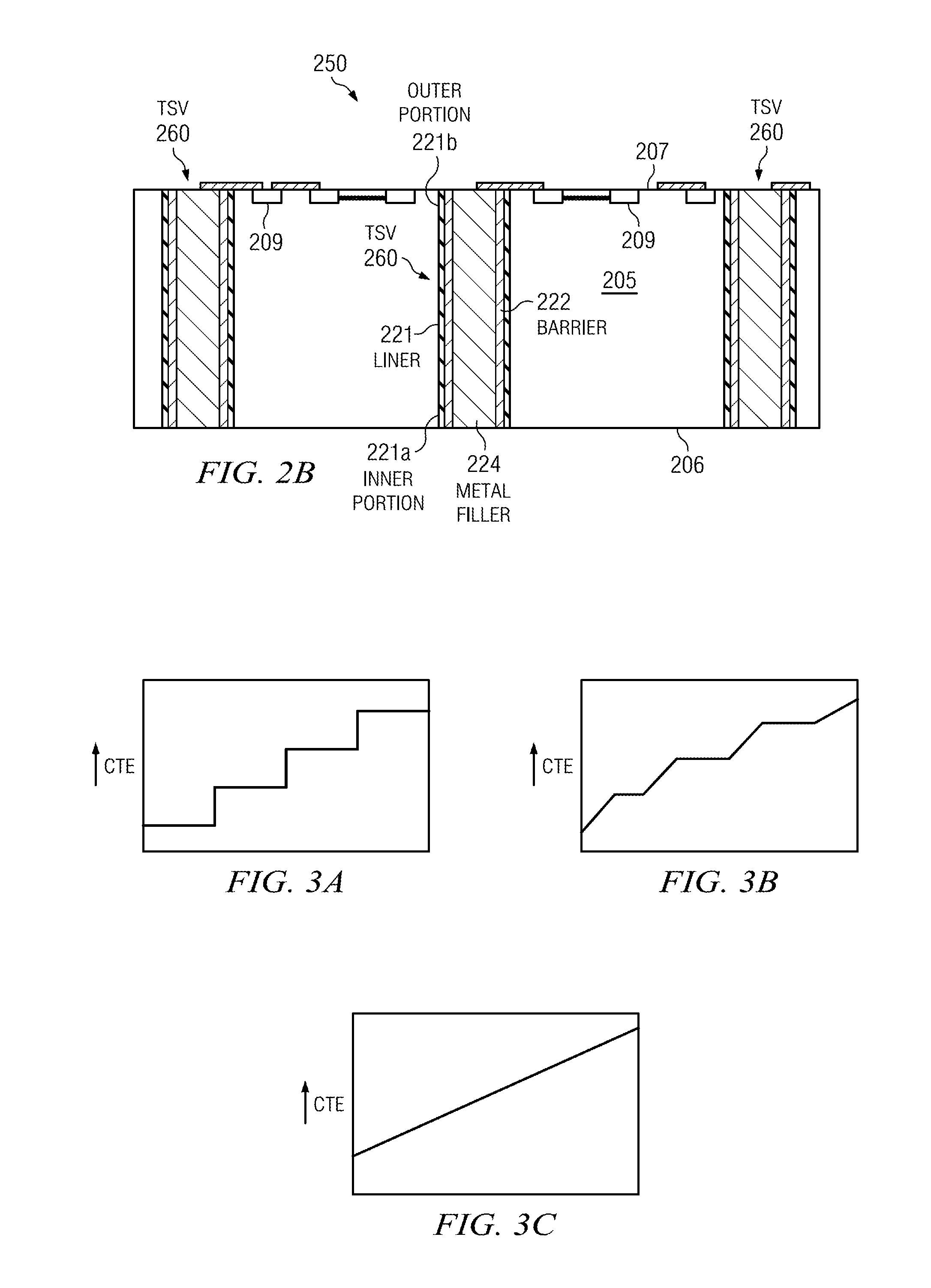
[0016]Disclosed embodiments include methods of fabricating a semiconductor die including disclosed CTE graded layers. FIG. 1 is a flow chart showing steps in an example method 100 of forming semiconductor die having multi-layer structures including disclosed CTE graded layers, according to an example embodiment. Step 101 comprises providing a substrate (e.g., a wafer) comprising a plurality of semiconductor die including a bottomside and a topside. Once method 100 and the other fabrication steps are completed, the topside will inc...


PUM


Abstract

A method of fabricating a semiconductor die includes circuit elements configured to provide a circuit function. A substrate including a bottomside and a topside is provided. At least one multi-layer structure is formed. The forming is done by depositing a coefficient of thermal expansion (CTE) graded layer comprising at least a dielectric portion on a first material having a first CTE to provide a first side facing said first material and a second side opposite the first side. The depositing includes flowing a first reactive component and at least a second reactive component. A gas flow ratio of the first reactive component relative to the second reactive component is automatically changed during a deposition time to provide a non-constant composition profile which has a graded CTE that increases from the first side to the second side. A metal layer comprising a second material having a second CTE is formed on the second side. The second CTE is higher than the first CTE.

Description

CROSS REFERENCE TO RELATED APPLICATIONS[0001]This application is a Divisional of and claims priority to U.S. patent application Ser. No. 13 / 251,498, filed on Oct. 3, 2011.FIELD[0002]Disclosed embodiments relate to semiconductor integrated circuit (IC) die including multi-layer structures that have significant coefficient of thermal expansion mismatches, such as through-silicon-vias.BACKGROUND[0003]Vias are routinely used in forming semiconductor ICs. Vias may be formed that extend vertically for the full die thickness from the bottomside of the die to one of the contact level or one of the metal interconnect levels, such as metal 1 on the active topside of the die. In the case of silicon substrates, such structures are often referred to as “through-silicon-vias”, and are referred to more generally herein as through-substrate-vias (TSVs). The TSV vertical electrical paths are significantly shortened relative to conventional wire bonding technology, generally leading to significantly ...

Claims


Application Information

Patent Timeline
IPC IPC(8): H01L21/768
CPCH01L21/76879H01L23/481H01L23/5329H01L23/53295H01L29/94H01L2924/0002H01L2924/00
Inventor KIRKPATRICK, BRIAN K.TIWARI, RAJESH
Owner TEXAS INSTR INC
Why Eureka
Try Eureka