Active Clamp Protection Circuit For Power Semiconductor Device For High Frequency Switching

a technology of active clamping and protection circuit, which is applied in the direction of electronic switching, emergency protective arrangements for limiting excess voltage/current, pulse technique, etc., can solve the problems of transistor device switching, transistor device discharging excessive power, transistor device down switching,

Active Publication Date: 2014-03-27
ALPHA & OMEGA SEMICON INC
View PDF7 Cites 39 Cited by
  • Summary
  • Abstract
  • Description
  • Claims
  • Application Information

AI Technical Summary

Benefits of technology

[0009]According to one embodiment of the present invention, a protection circuit for a power transistor having a first terminal configured to drive a load, a second terminal coupled to a first power supply voltage, and a control terminal configured to receive a control signal, includes a first transistor having a first terminal coupled to the first terminal of the power transistor, a second terminal coupled to the first power supply voltage, and a control terminal coupled to the first power supply voltage through a first resistive element; and a first set of diodes connected between the first terminal and the control terminal of the first transistor. In operation, a voltage between the first terminal and the control terminal of the first transistor is clamped at a voltage sum of all diode voltages of the first set of diodes, the diode voltages including forward voltage or reverse voltage. The first transistor is turned on to conduct current in a forward conduction mode when an over-voltage condition occurs at the first terminal of the power transistor.

Problems solved by technology

Without any circuit protection, the parasitic bipolar transistor may turn on and irreversible damages to the transistor device may result.
As a result, the transistor dissipates the excessive power due to inductive fly-back in the conduction mode with the power transistor being turned on, rather than in the more undesirable avalanche mode when the power transistor is turned off.
However, such gate resistance slows down the switching of the transistor device, rendering the device not suitable for high speed switching applications.

Method used


Image

  • Active Clamp Protection Circuit For Power Semiconductor Device For High Frequency Switching
  • Active Clamp Protection Circuit For Power Semiconductor Device For High Frequency Switching
  • Active Clamp Protection Circuit For Power Semiconductor Device For High Frequency Switching

Examples


Embodiment Construction

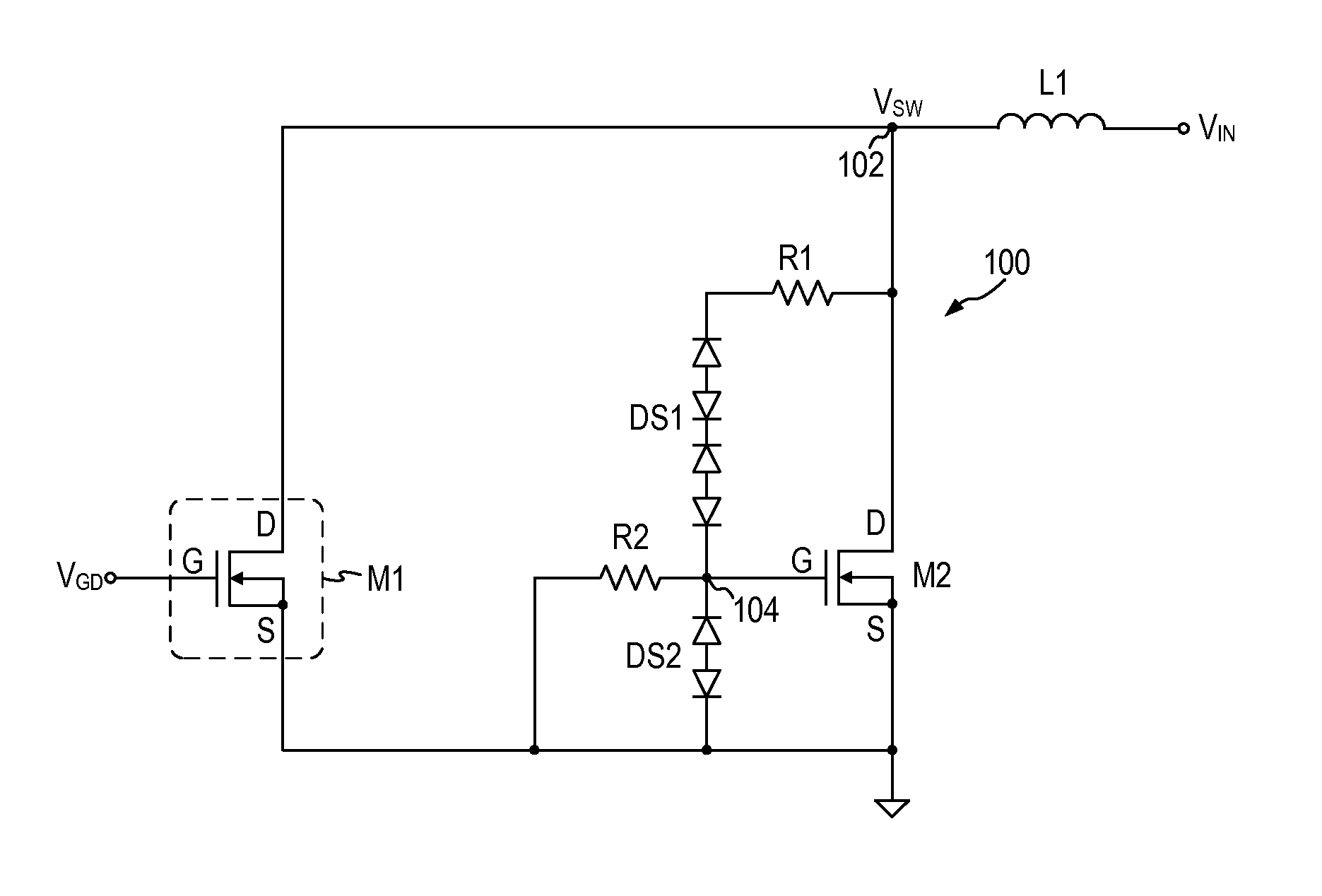
[0018]In accordance with the principles of the present invention, an active clamp protection circuit for a power transistor switching an inductive load includes a grounded active clamp transistor connected in parallel with the protected power transistor. The active clamp transistor has its gate terminal tied to the ground potential through a resistor so that the active clamp transistor remains turned off during normal operation but is turned on during an Unclamped Inductive Switching (UIS) event to absorb the inductor energy. In this manner, the gate terminal of the protected power transistor can be connected directly to the gate drive signal without intervening gate resistance that may slow down the switching speed of the power transistor.

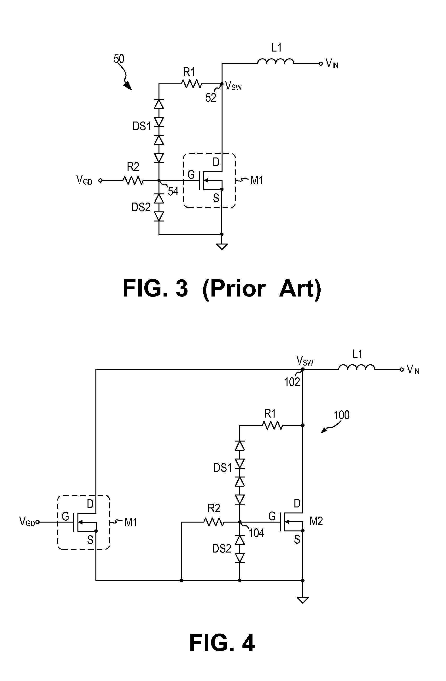
[0019]FIG. 3 is a circuit diagram illustrating a typical active clamp protection circuit as applied to protect a power transistor. Referring to FIG. 3, a power transistor M1, which is a MOSFET in the present illustration, is configured to switch a...


PUM


Abstract

A protection circuit for a power transistor includes a first transistor connected in parallel with the power transistor and having a control terminal connected to a first power supply voltage through a first resistive element; and a first set of diodes connected between a first terminal and a control terminal of the first transistor. In operation, the voltage at the first terminal of the first transistor is clamped to a clamp voltage and the first transistor is turned on to conduct current in a forward conduction mode when an over-voltage condition occurs at a first terminal of the power transistor.

Description

FIELD OF THE INVENTION[0001]The invention relates to protective circuits for power semiconductor devices and, in particular, to an active clamp protection circuit for protecting a power semiconductor device while enabling high frequency switching operation.DESCRIPTION OF THE RELATED ART[0002]Power transistors, such as power MOSFETs, are often used in applications for switching an inductive load. Such power transistors may include a protection circuit integrated therewith for protecting the transistor against short-circuit events at the load, against drain over-voltage conditions, and against electrostatic discharge (ESD). For a power MOSFET, the protection circuit may also include current limiting elements to protect the transistor from damages caused by operating outside the safe operating area. The protection circuit may further include over-voltage protection circuit at the drain terminal to protect the MOSFET from damages caused by over-voltage transients.[0003]In particular, wh...

Claims


Application Information

Patent Timeline
Patent Type & Authority Applications(United States)
IPC IPC(8): H02H3/20
CPCH03K17/0822H01L27/0255H01L27/0266H03K17/08
Inventor LUI, SIK K.
Owner ALPHA & OMEGA SEMICON INC
Why Eureka
Try Eureka