Solar cell and method for producing same

a solar cell and cell technology, applied in the field of solar cells and methods for producing same, can solve the problems of lack of cheap mass, use of expensive photolithography processing steps,

Active Publication Date: 2014-04-10
REC SOLAR
View PDF9 Cites 22 Cited by
  • Summary
  • Abstract
  • Description
  • Claims
  • Application Information

AI Technical Summary

Benefits of technology

[0048]In an embodiment, the mask is made of a material with a coefficient of thermal expansion same or close to that of the silicon substrate. Using a mask with such corresponding thermal expansion coefficient, any misalignment of the mask with respect to the silicon substrate due to thermal expansion during heating-up for a layer sequence deposition process may be minimized.
[0049]It may be noted that possible features and advantages of embodiments of the present invention are described herein with respect to the proposed rear contact heterojunction solar cell or with respect to the proposed method for fabricating such solar cell. One skilled in the art will recognize that the different features may be arbitrarily combined and features of the solar cell may be realized in a corresponding manner in the fabricating method and vice versa in order to implement further advantageous embodiments and realize synergetic effects.

Problems solved by technology

For example, it has been proposed to use expensive photolithography processing steps to precisely define areas of semiconductor layers or insulator layers on the substrate's rear surface.
However, it seems that all conventional approaches for generating a rear contact heterojunction intrinsic thin film solar cell scheme suffer from at least one of the following shortcomings:a lack of a cheap mass-production methodpoor passivation at electrode edges due to imperfect definition of electrode areasa risk of shunting forcing metallization only over a limited part of the electrodesdifficulties in controlling the cleanness and deposition homogeneity of the intrinsic thin film in the critical layer closest to the substrateexpensive layer geometry definition due to the use of lithographya requirement of using -orientated silicon wafers as substrates.

Method used


Image

  • Solar cell and method for producing same
  • Solar cell and method for producing same
  • Solar cell and method for producing same

Examples


Embodiment Construction

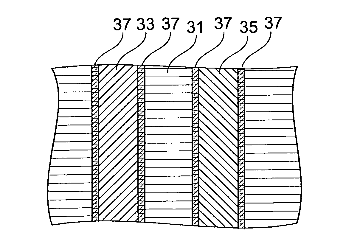
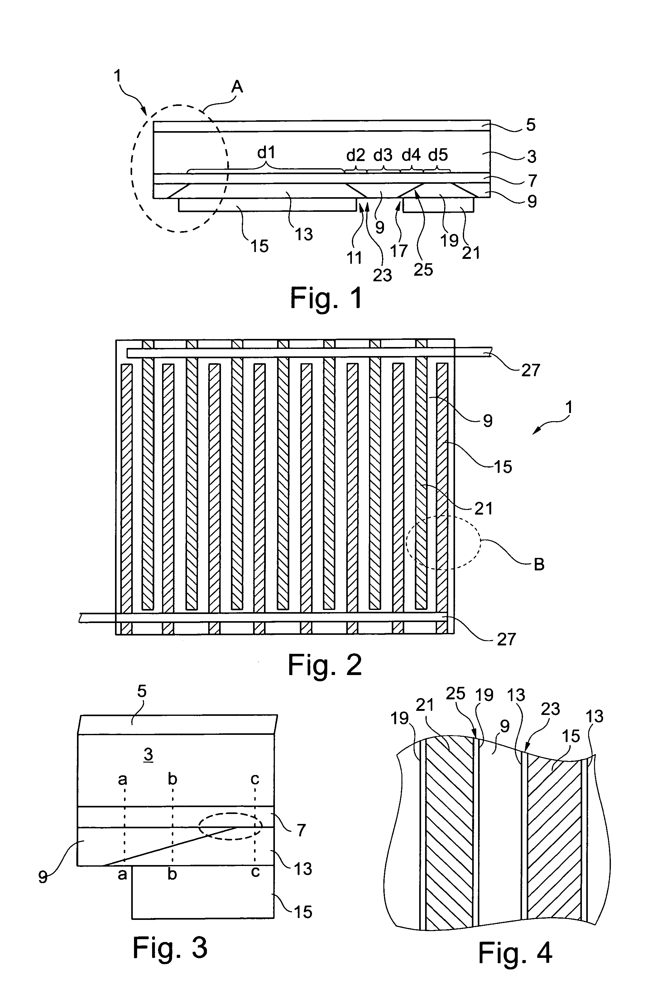
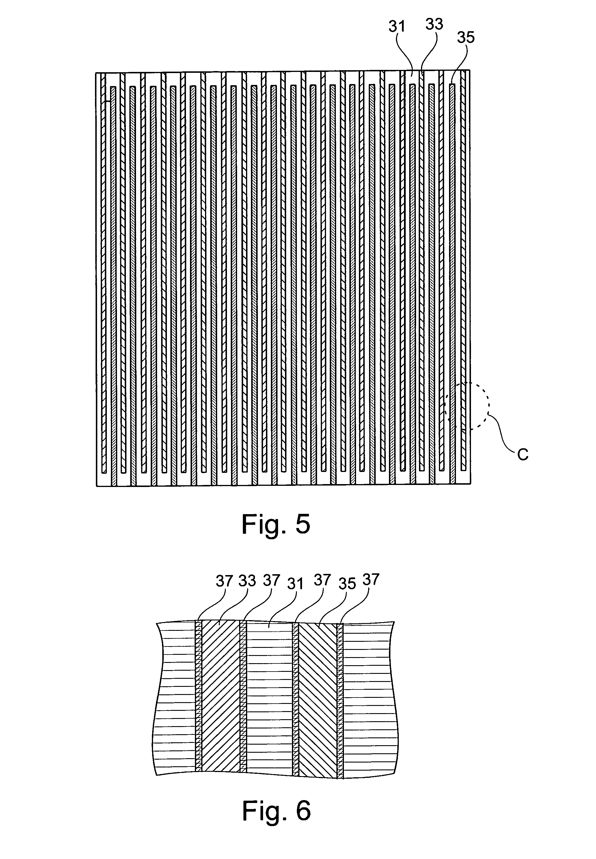
[0060]An objective of embodiments of the present invention is to provide a cost effective, industrially applicable method for fabricating back-contacted silicon heterojunction intrinsic-thin layer solar cells, and a detailed solar cell design adapted to and resulting from such a fabricating method.

[0061]In the back-contacted silicon heterojunction intrinsic-thin layer solar cells, the intrinsic layer has to be thin enough to allow tunnelling, but thick enough to passivate the adjacent silicon surface. This means that both a very low defect density and an absolute thickness control are essential. Any method that allows depositing the intrinsic layer for the entire rear surface in one go therefore has huge benefits for ease of optimization and process control in production, and is likely to have a higher maximum efficiency potential.

[0062]All existing methods for producing similar solar cells include etching through, and partially rebuilding this layer, or etching down to the layer, w...


PUM


Abstract

A rear contact heterojunction solar cell and a fabricating method. The solar cell comprises a silicon substrate having a passivating layer and an intrinsic amorphous silicon layer. At a back side of the intrinsic amorphous silicon layer, an emitter layer and a base layer are provided. Interposed between these emitter and base layers is a separation layer comprising an electrically insulating material. This separation layer as well as the base layer and emitter layer may be generated by vapour deposition. Due to such processing, adjacent regions of the emitter layer and the separating layer and adjacent regions of the base layer and the separating layer partially laterally overlap in overlapping areas in such a way that at least a part of the separating layer is located closer to the substrate than an overlapping portion of the respective one of the emitter layer and the base layer.

Description

FIELD OF THE INVENTION[0001]The present invention relates to a rear contact heterojunction intrinsic thin layer silicon solar cell and a method for fabricating such solar cell.TECHNICAL BACKGROUND[0002]Solar cells are used to convert sunlight into electricity using a photovoltaic effect. A general object is to achieve high conversion efficiency balanced by a need for low production costs.[0003]In order to obtain high efficiency, semiconductor materials of good quality should be used as substrates for the solar cell and the surfaces of the substrates should be highly passivated in order to minimize any recombination losses. Furthermore, contact schemes for electrically contacting the substrate should be optimized in order to minimize resistance losses and shading.[0004]In order to keep production costs low, it is generally intended to use as few processing steps as possible and furthermore to prevent complicated and costs-intensive production steps such as e.g. photolithography maski...

Claims


Application Information

Patent Timeline
Patent Type & Authority Applications(United States)
IPC IPC(8): H01L31/074H01L31/075H01L31/18
CPCH01L31/074H01L31/075H01L31/18H01L31/022441H01L31/0747Y02E10/548H01L31/022425Y02E10/50H01L31/0224H01L31/04
Inventor KIRKENGEN, MARTINSAUAR, ERIK
Owner REC SOLAR
Why Eureka
Try Eureka