Semiconductor device and method for manufacturing the same

Active Publication Date: 2014-04-17
SEMICON ENERGY LAB CO LTD
View PDF2 Cites 30 Cited by
  • Summary
  • Abstract
  • Description
  • Claims
  • Application Information

AI Technical Summary

Benefits of technology

[0018]According to one embodiment of the present invention, electrical characteristic variation of a semiconductor device including an oxide semiconductor layer can be reduced. Fur

Problems solved by technology

When oxygen vacancies are generated in the side surface of the oxide semiconductor layer, the resistance of the side surface is reduced and an apparent threshold voltage of the transistor is changed, which causes a problem that threshold-voltage variat

Method used


Image

  • Semiconductor device and method for manufacturing the same
  • Semiconductor device and method for manufacturing the same
  • Semiconductor device and method for manufacturing the same

Examples


example 1

[0555]In this example, a transistor using a multilayer film including an oxide semiconductor layer was formed and cross-sectional observation with an electron microscope and measurement of electrical characteristics were performed.

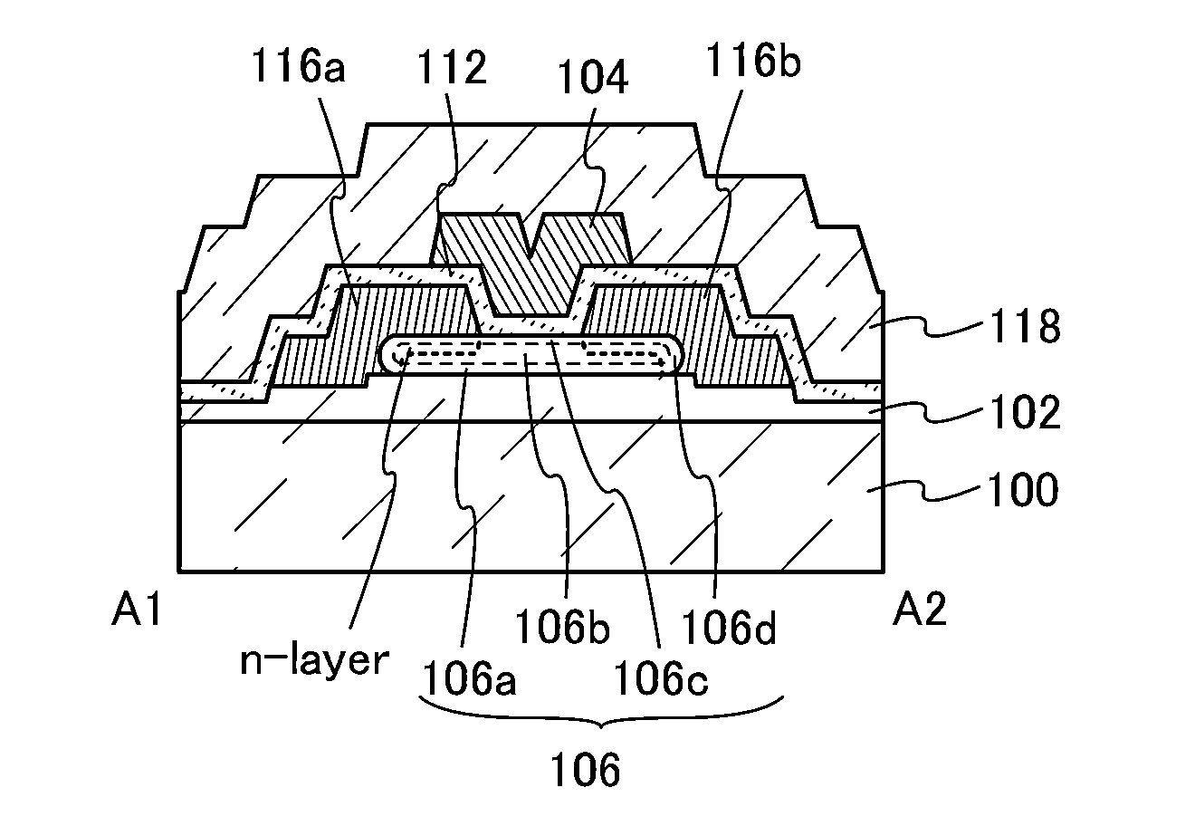
[0556]Example Sample 1 and Example Sample 2 were prepared in the following manner. Note that Example Sample 1 and Example Sample 2 are each a TGTC transistor illustrated in FIGS. 21A to 21D. Accordingly, hereinafter, the descriptions using FIGS. 3A to 3C, FIG. 4A to 4C, FIGS. 5A and 5B, FIGS. 21A to 21D, FIGS. 24A to 24C, FIGS. 25A and 25B, and the like are referred to for Example Sample 1 and Example Sample 2.

[0557]First, Example Sample 1 is described.

[0558]A glass substrate was used as the substrate 100.

[0559]As the base insulating film 102, a silicon oxynitride film was used.

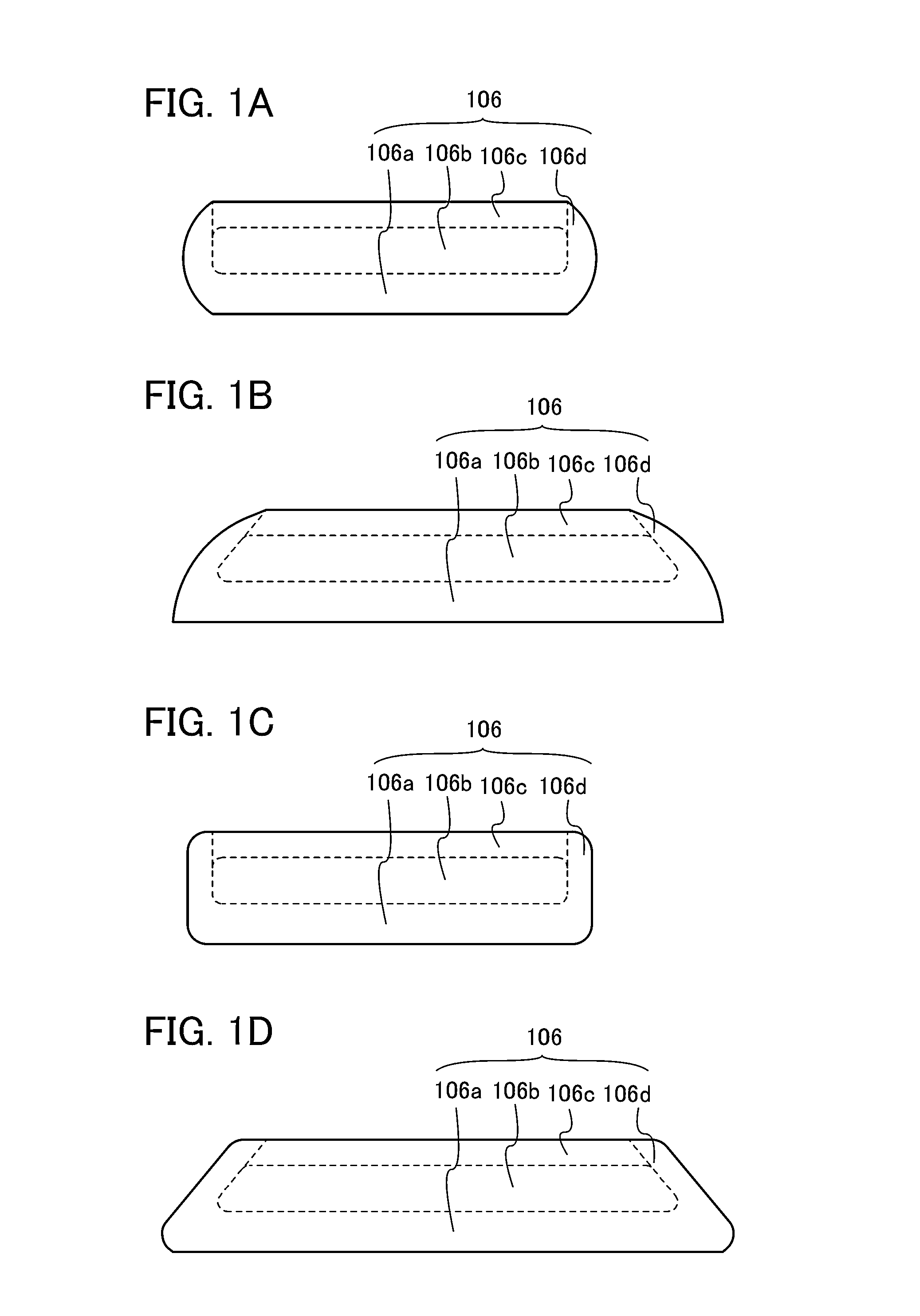
[0560]A method for forming the oxide layer 106a, the oxide semiconductor layer 106b, the oxide layer 106c, and the oxide layer 106d is described below.

[0561]First, as the oxide laye...


PUM


Abstract

A semiconductor device formed using an oxide semiconductor layer and having small electrical characteristic variation is provided. A highly reliable semiconductor device including an oxide semiconductor layer and exhibiting stable electric characteristics is provided. Further, a method for manufacturing the semiconductor device is provided. In the semiconductor device, an oxide semiconductor layer is used for a channel formation region, a multilayer film which includes an oxide layer in which the oxide semiconductor layer is wrapped is provided, and an edge of the multilayer film has a curvature in a cross section.

Description

TECHNICAL FIELD[0001]The present invention relates to a semiconductor device and a method for manufacturing the semiconductor device.[0002]In this specification, a semiconductor device generally means a device which can function by utilizing semiconductor characteristics, and an electrooptic device, a semiconductor circuit, and electronic equipment are all semiconductor devices.BACKGROUND ART[0003]Attention has been focused on a technique for forming a transistor using a semiconductor thin film (also referred to as a thin film transistor (TFT)). Such a transistor is applied to a wide range of electronic devices such as integrated circuits (ICs) or image display devices. A silicon-based semiconductor material is widely known as a material for a semiconductor thin film applicable to a transistor. As another material, an oxide semiconductor has been attracting attention.[0004]For example, a transistor including an amorphous oxide containing indium (In), gallium (Ga), and zinc (Zn) as a...

Claims


Application Information

Patent Timeline
IPC IPC(8): H01L29/786H01L29/66H01L29/26
CPCH01L29/78693H01L29/66969H01L29/263H01L21/02554H01L21/02565H01L21/0262H01L21/02631H01L29/78696H01L21/467H01L21/477H01L29/247
Inventor YAMAZAKI, SHUNPEISUZAWA, HIDEOMI
Owner SEMICON ENERGY LAB CO LTD
Why Eureka
Try Eureka