Method and apparatus for testing interconnection reliability of a ball grid array on a testing printed circuit board

a technology of interconnection reliability and printed circuit board, which is applied in the direction of individual semiconductor device testing, instruments, solid-state devices, etc., can solve the problems of increasing cost and time in the overall fabrication process, limited reliability tests, and limited testing of connection bga

Active Publication Date: 2014-04-24
NVIDIA CORP
View PDF10 Cites 22 Cited by
  • Summary
  • Abstract
  • Description
  • Claims
  • Application Information

AI Technical Summary

Problems solved by technology

In such cases, reliability tests are often limited to the power cycling and some kind of thermal cycling and vibration and the testing of connection BGA is very limited.
To address this issue, the testing of the...

Method used


Image

  • Method and apparatus for testing interconnection reliability of a ball grid array on a testing printed circuit board
  • Method and apparatus for testing interconnection reliability of a ball grid array on a testing printed circuit board
  • Method and apparatus for testing interconnection reliability of a ball grid array on a testing printed circuit board

Examples


Embodiment Construction

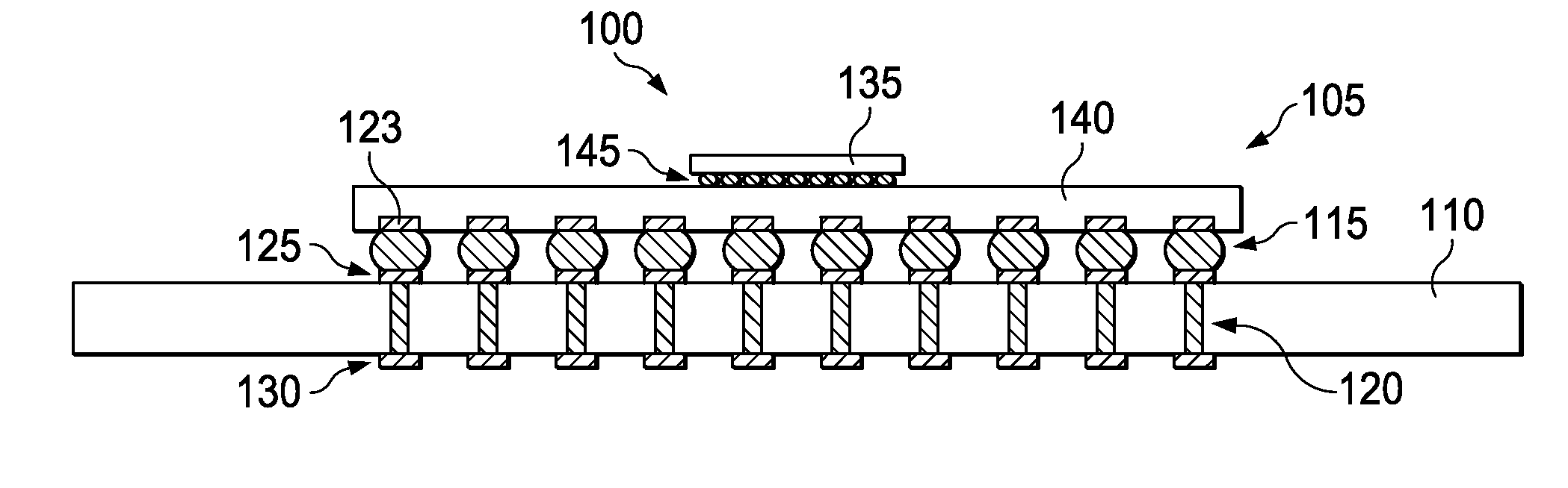
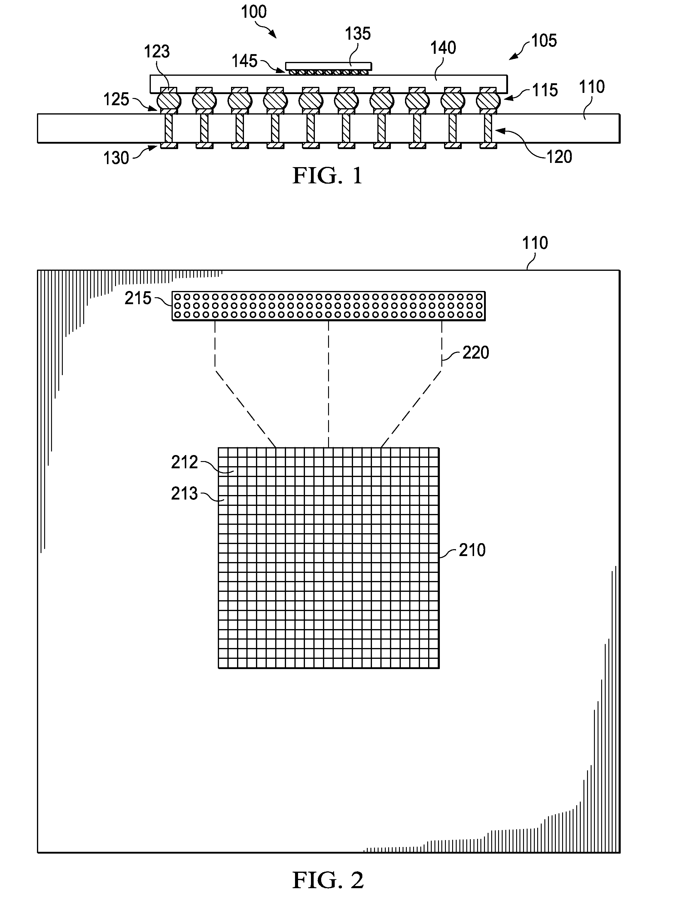
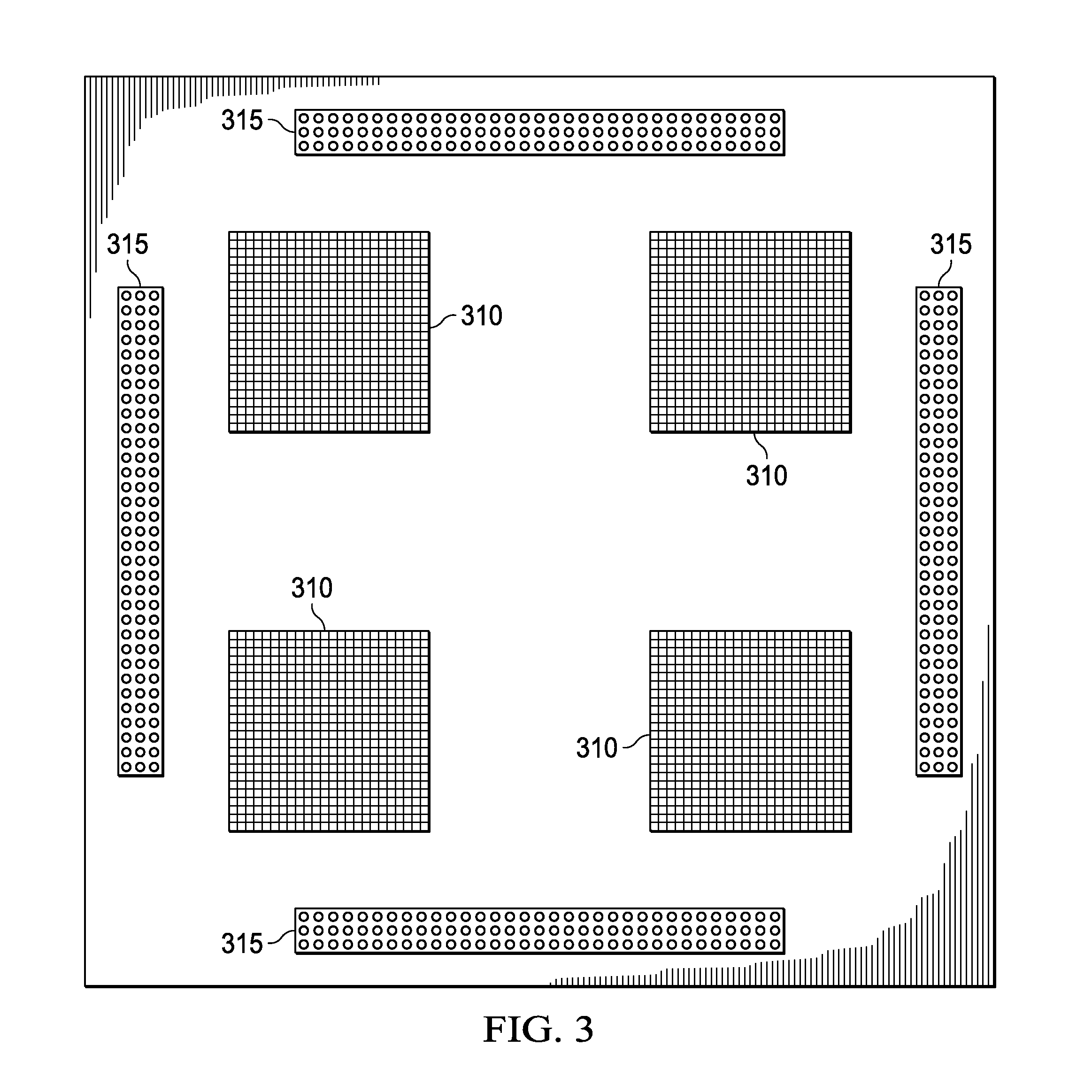
[0013]The present disclosure is directed to a method and system for testing the reliability of solder joints in an IC package assembly that includes an IC device and that is connected to a testing PCB by a BGA. The present disclosure offers advantages over conventional methods and apparatus in that the testing PCB does not have to be re-designed, as is the case with daisy chained boards. Moreover, the testing PCB can be standardized to test different types of IC packages and IC devices and multiple IC packages at the same time. Additionally, it does not involve the costly and time-consuming steps of producing a completed circuit board with all the peripheral components and circuits associated with it, such as a graphics card or motherboard. Thus, the product development cycle and the system / board level qualification can be significantly reduced by several months, and the cost of the board level qualification can be significantly reduced, as well. Another advantage provided by the pr...


PUM


Abstract

An apparatus for determining an electrical reliability of a ball grid array (BGA) assembly of an integrated circuit is presented. The assembly comprises a testing printed circuit board (PCB) having an integrated circuit (IC) test region located thereon. Vias extend through the testing PCB from a surface to an underside thereof within the IC test region. Each via has an IO pad or ground pad electrically connectable thereto. An IC package having an IC die connected thereto by solder bumps is connected to the IC test region by solder balls, such that each of the IO pads is electrically connectable to a respective pair of the solder balls and solder bumps by the vias. A method of testing interconnection reliability of the BGA using the apparatus is also presented.

Description

TECHNICAL FIELD[0001]This application is directed, in general, to a method and apparatus for testing interconnection reliability of a ball grid array (BGA) on a testing printed circuit board (PCB).BACKGROUND[0002]Integrated circuit (IC) devices typically included an IC chip housed in an IC “package” that typically includes a plastic, ceramic, or metal substrate. The IC chip includes an IC formed on a thin wafer of silicon. The IC package supports and protects the IC chip and provides electrical connections between the IC and an external circuit or system. Typically, the IC package is connected to a PCB by way of solder balls that form a BGA.[0003]To ensure consistent quality, IC manufacturers typically test their IC devices thoroughly before shipping to customers. Part of this IC testing determines if the IC device is functional, and the results of these tests provide customers operating characteristics that are used by the customers in designing their systems. Another portion of th...

Claims


Application Information

Patent Timeline
IPC IPC(8): G01R31/26
CPCG01R31/2853G01R1/0408G01R31/048H01L2224/16227H01L2224/16235H01L2924/15311G01R31/71
Inventor XIE, DONGJIWOO, MIN
Owner NVIDIA CORP
Why Eureka
Try Eureka