
Laminated busbar for power converter and the converter thereof

a power converter and busbar technology, applied in the direction of busbar installation, electric cable installation, electrical apparatus construction details, etc., can solve the problems of increasing voltage stress on the semiconductor component, reducing reliability and even damaging the semiconductor component, and additional turning-on loss, etc., to achieve the effect of convenient installation

Active Publication Date: 2014-04-24
DELTA ELECTRONICS INC
View PDF7 Cites 65 Cited by
  • Summary
  • Abstract
  • Description
  • Claims
  • Application Information

AI Technical Summary

Benefits of technology

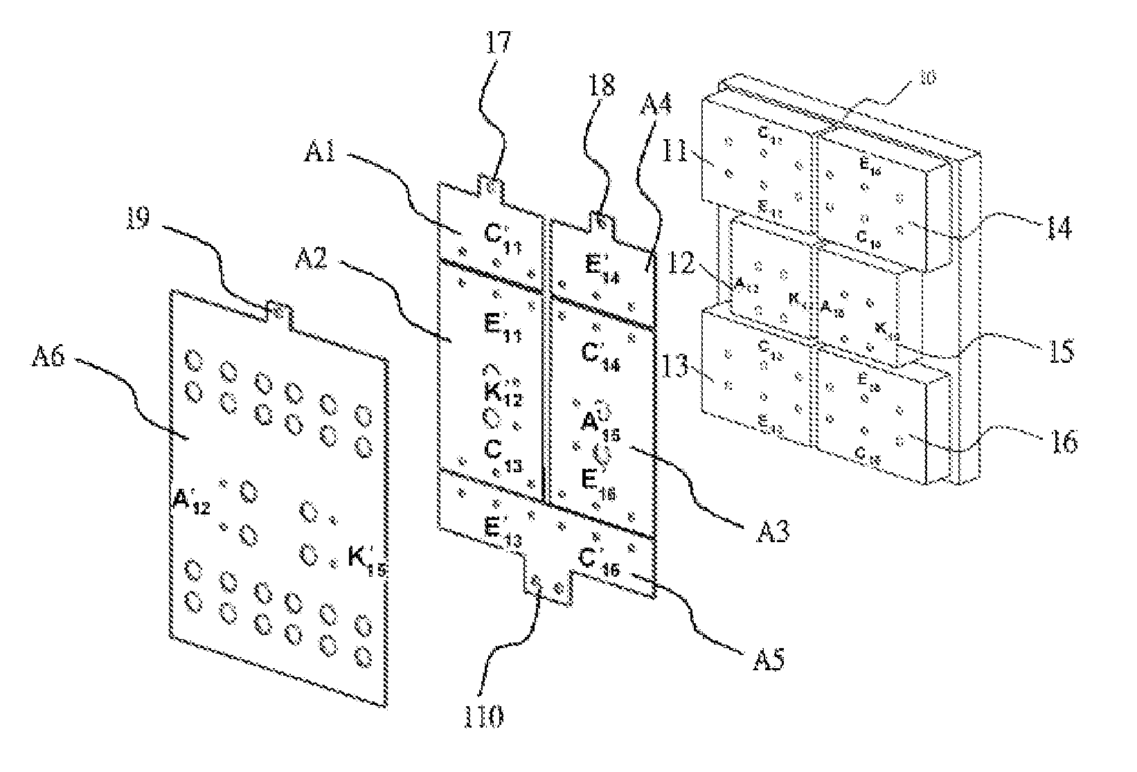
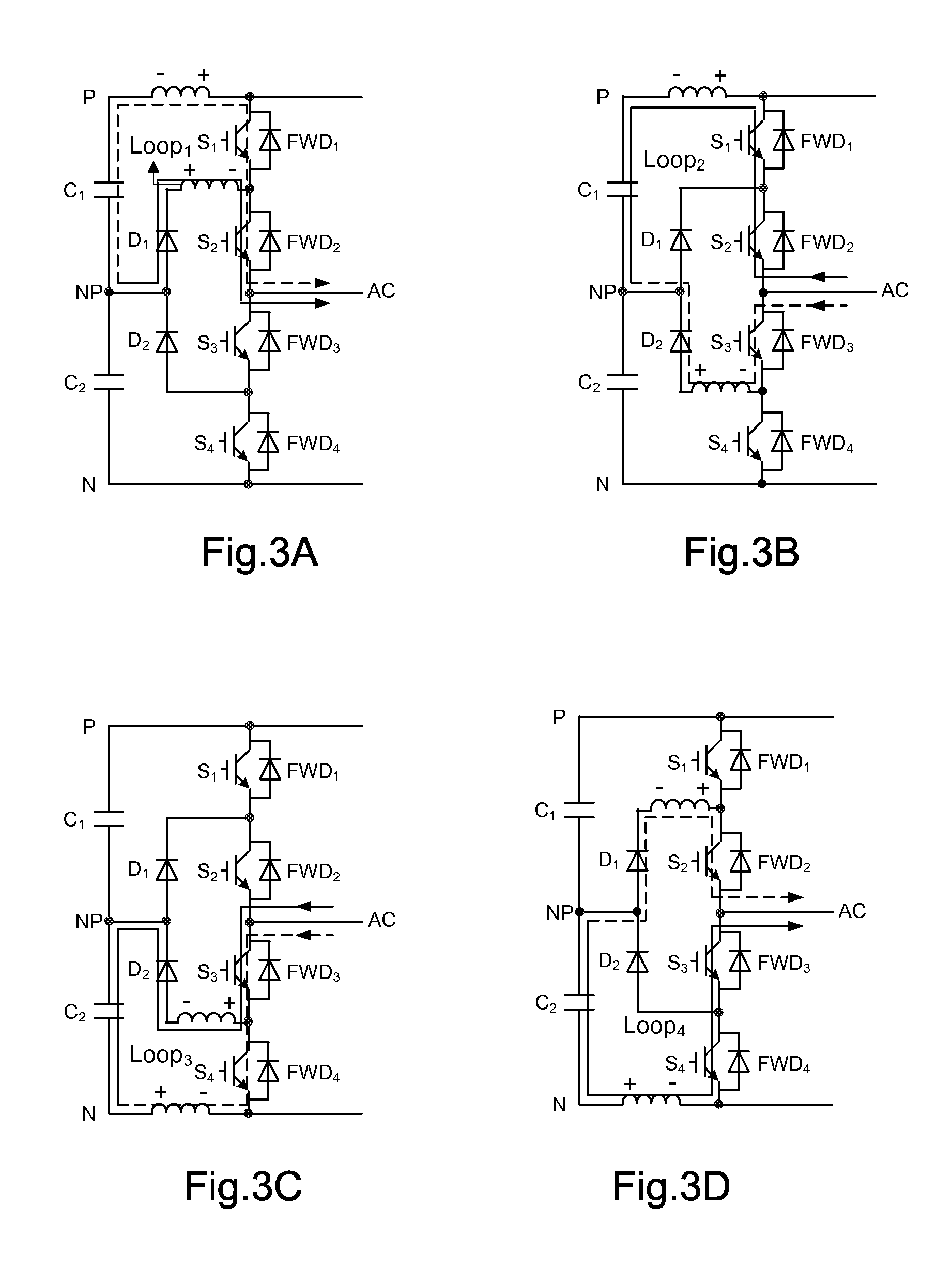
The present invention aims to provide a laminated busbar for a three-level power converter that reduces stray inductance, has a simple structure, and is easy to install. The invention also provides a mirror path for currents flowing through the circuit at commutation step, which results in reduced voltage stress and efficient reduction of stray inductance.

Problems solved by technology

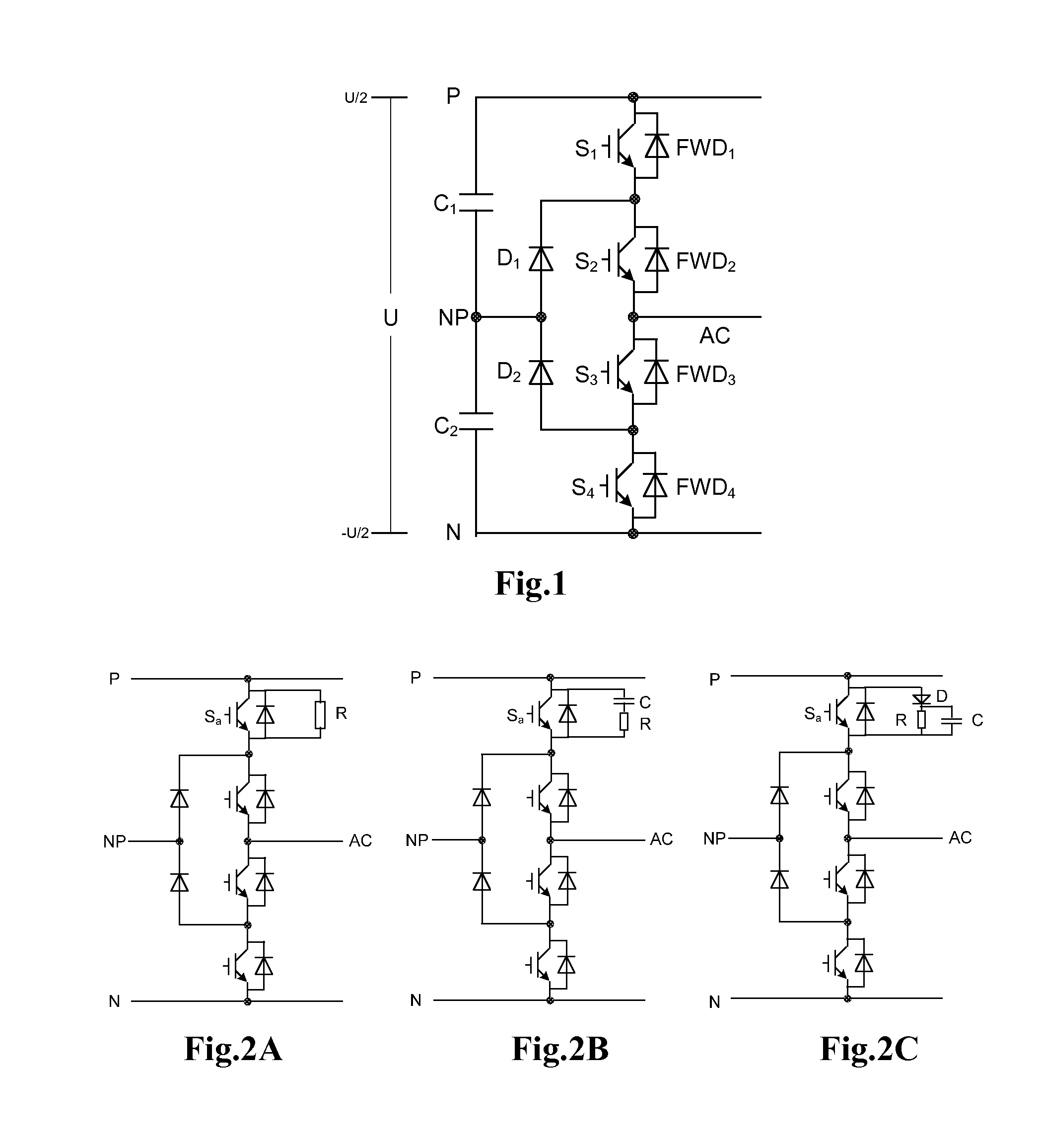
In particular, as switching speed of semiconductor components and power output are increasingly improved, stray inductance induces a high voltage when a semiconductor component turns off under normal operation or short-circuit, which may increase voltage stress to the semiconductor component, thereby reducing reliability and even damaging the semiconductor component.
Although this method can reduce the influence simply and effectively, when S1 is turned on, energy absorbed by the snubber circuit is released through S1, which leads to additional turned-on loss and deteriorates dynamic performance of semiconductor components.
In addition, since additional high voltage devices are added, the converter has disadvantages of an increased failure rate, a reduced power density, an improved cost, and so on.
Although stray inductance can be approximately ignored when laminated busbar used, some other problems still exist in such laminated busbars in the art.
For example, particularly in the NPC three-level circuit, since the number of components increases, and the area of components itself increases, multiple layers of laminated busbars are required to achieve so complicated electrical connection, and the manufacturing cost of such multiple layers of laminated busbars becomes high.
In addition, as the layer number of busbars increases, stray inductance increases due to the increasing thick of insulating layers located between layers, and the insulating process between layers becomes more complicated.
In addition, in this patent, the shapes of respective sub busbars are different from each other, and it is required to process bendings and steps with different depths in respective layers so as to connect each of layer of busbar with corresponding pins of semiconductor components, which makes the manufacturing process of busbar complicated, and it is necessary to make adherence processing between the respective busbars so as to avoid gaps between laminated layers due to bending of busbar.
Therefore, the electrical performance of such busbar structure is weak and counts against cost optimization.
Thus, there exist such problems that the layer number of busbars is too many to weaken the effect of the realization of low stray inductance, it is required to process different holes since the shapes of respective sub busbars are different from each other, and too many laminated layers needs to more holes (more through holes).
Therefore, the laminated busbar proposed by this patent is also complicated and counts against cost optimization.

Method used


Image

  • Laminated busbar for power converter and the converter thereof
  • Laminated busbar for power converter and the converter thereof
  • Laminated busbar for power converter and the converter thereof

Examples


first embodiment

A First Embodiment

[0061]As shown in FIG. 4A, an upper arm in one phase of the circuit of a power converter having a NPC three-level topology comprises semiconductor components S11 and S13, freewheeling diodes FWD11 and FWD13 respectively connected in parallel with S11 and S13, and a lower arm thereof comprises semiconductor components S14 and S16, freewheeling diodes FWD14 and FWD16 respectively connected in parallel with S14 and S16. A terminal of a clamping diode D12 is connected to S11 and S13 of the upper arm, and the other terminal thereof is connected to a neutral-point potential. A terminal of a clamping diode D15 is connected to S14 and S16 of the lower arm, and the other terminal thereof is connected to the neutral-point potential. An upper-arm busbar capacitor C110 is connected in series between a positive DC input and the neutral-point potential, and a lower-arm busbar capacitor C120 is connected in series between a negative DC input and the neutral-point potential. In FI...

second embodiment

A Second Embodiment

[0084]As shown in FIG. 8A, in this embodiment, S211, S221, S222 and S232 are semiconductor components, FWD211, FWD221, FWD222 and FWD232 are freewheeling diodes, FWD212 and FWD231 are clamping diodes, C210 is an upper-arm busbar capacitor, and C220 is a lower-arm busbar capacitor.

[0085]The difference between the second embodiment and the first embodiment lies in that there are only three the semiconductor modules. In this embodiment, the semiconductor components S211, FWD211 and FWD212 constitute a semiconductor module 21, the semiconductor components S221, FWD221, D221, S222 and FWD222 constitute a semiconductor module 22, and the semiconductor components S232, FWD231 and FWD232 constitute a semiconductor module 23. The plurality of semiconductor modules form a power unit component group 211.

[0086]As shown in FIG. 8B, the power unit component group 211 comprises semiconductor module 21, 22 and 23, which are located in the same plane. All of the semiconductor modu...


PUM


Abstract

The present application discloses a laminated busbar arrangement for use in a three-level power converter and a power converter. The laminated busbar arrangement comprises a first layer of busbar comprising a neutral-point sub busbar congfigured to make electrical connections between respective components in the three-level power converter and a neutral-point potential; a second layer of busbar comprising a plurality of sub busbars congfigured to make electrical connections between the respective components in the three-level power converter and a positive direct current (DC) input, a negative DC input and an alternating current (AC) input / output in the three-level power converter, and between respective semiconductor switching components. The present application may effectively reduce stray inductance.

Description

CROSS-REFERENCE TO RELATED APPLICATIONS[0001]The present application claims priority under 35 U.S.C. §119 to Chinese Patent Application No. 201210403971.1, filed on Oct. 22, 2012, the entire contents of which are incorporated herein by reference.TECHNICAL FIELD[0002]The present application relates to a laminated busbar, and particularly to a laminated busbar structure having two layers of busbars and a NPC (neutral-point clamp) three-level power converter with the laminated busbar.BACKGROUND ART[0003]Presently, variable frequency converters are widely used in industry fields and are tending to be developed to high voltage, large current, high power density, high reliability and low cost. In high voltage variable frequency field, since the power converter is restricted by the performance of semiconductor components, a NPC three-level topology is generally used.[0004]FIG. 1 is a circuit diagram showing one phase of the circuit of a typical NPC three-level topology. Although FIG. 1 onl...

Claims


Application Information

Patent Timeline
IPC IPC(8): H05K7/02
CPCH05K7/026H02M7/003H02M7/487H02M1/348H05K7/14329
Inventor LI, YANGAN, HONGJIANWEN, SENLINYING, JIANPING
Owner DELTA ELECTRONICS INC
Learn More