ALIGNMENT OF SINGLE-MODE POLYMER WAVEGUIDE (PWG) ARRAY AND SILICON WAVEGUIDE (SiWG) ARRAY FOR PROVIDING ADIABATIC COUPLING

a technology of adiabatic coupling and polymer waveguide, which is applied in the direction of photomechanical equipment, instruments, originals for photomechanical treatment, etc., can solve the problems of not being able to provide adiabatic coupling or refer to high-precision alignment, and difficult to use butt coupling

Active Publication Date: 2014-04-24
GLOBALFOUNDRIES US INC
View PDF2 Cites 33 Cited by
  • Summary
  • Abstract
  • Description
  • Claims
  • Application Information

AI Technical Summary

Benefits of technology

[0011]The present invention allows high-precision alignment of a single-mode polymer waveguide (PWG) array fabricated on a polymer and a silicon waveguide (SiWG) array fabricated on a silicon (Si) chip, so that an adiabatic coupling is realize...

Problems solved by technology

Thus, it is very difficult to use the Butt Coupling.
However, there is no known literature which provides the a...

Method used


Image

  • ALIGNMENT OF SINGLE-MODE POLYMER WAVEGUIDE (PWG) ARRAY AND SILICON WAVEGUIDE (SiWG) ARRAY FOR PROVIDING ADIABATIC COUPLING
  • ALIGNMENT OF SINGLE-MODE POLYMER WAVEGUIDE (PWG) ARRAY AND SILICON WAVEGUIDE (SiWG) ARRAY FOR PROVIDING ADIABATIC COUPLING
  • ALIGNMENT OF SINGLE-MODE POLYMER WAVEGUIDE (PWG) ARRAY AND SILICON WAVEGUIDE (SiWG) ARRAY FOR PROVIDING ADIABATIC COUPLING

Examples


Embodiment Construction

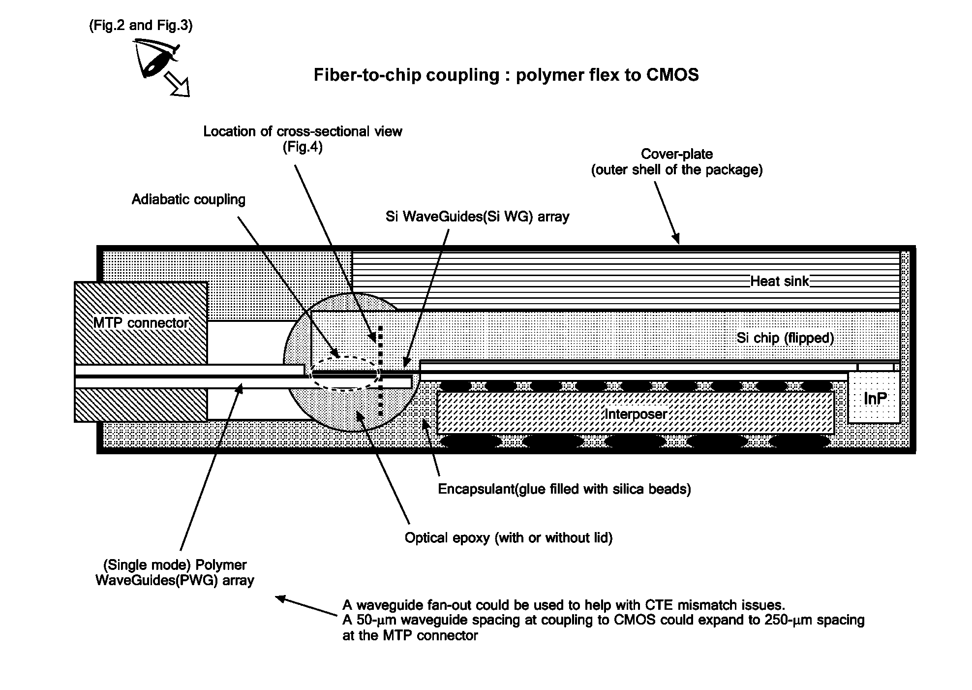
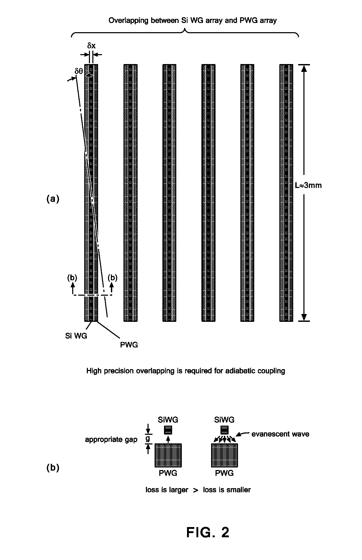
[0031]The present invention allows high-precision alignment of a single-mode polymer waveguide (PWG) array fabricated on a polymer and a silicon waveguide (SiWG) array fabricated on a silicon (Si) chip so that an adiabatic coupling is realized. A single-mode polymer waveguide (PWG) array fabricated on polymer and a silicon waveguide (SiWG) array fabricated on a silicon (Si) chip are self-aligned according to a combination of a stub and a groove highly precisely fabricated on both sides.

[0032]FIG. 1 is an overall view illustrating an area in which the inventive adiabatic coupling is provided and the structure of a package containing the area.

[0033]Adiabatic coupling is realized by aligning a single-mode polymer waveguide (PWG) array fabricated on a polymer with a silicon waveguide (SiWG) array fabricated on a silicon (Si) chip. The combined coupling portions in which this adiabatic coupling is provided are secured by an optical epoxy or a UV adhesive.

[0034]Further included are an MTP...


PUM

PropertyMeasurementUnit
Fractionaaaaaaaaaa
Fractionaaaaaaaaaa
Widthaaaaaaaaaa

Abstract

Alignment of a single-mode polymer waveguide (PWG) array fabricated on a polymer with a silicon waveguide (SiWG) array fabricated on a silicon (Si) chip and thereby realizing an adiabatic coupling. A stub and a groove are fabricated with high precision and made to function as the absolute positioning reference to provide a self-alignment according to the groove and the stub. In a PWG patterning by photolithography, plural masks are used, but the fabrication is made along the alignment base line for mask and thus a high precision is achieved with respect to error δx. In a PWG patterning by nano imprint, a high precision in the fabrication is also achieved with respect to error δx and δy.

Description

CROSS-REFERENCE TO RELATED APPLICATION[0001]This application claims priority under 35 U.S.C. §119 from Japanese Patent Application No. 2012-231090 filed Oct. 18, 2012, the entire contents of which are incorporated herein by reference.BACKGROUND OF THE INVENTION[0002]The present invention relates to the provision of a coupling allowing transmission of light between a polymer waveguide (PWG) array and a silicon waveguide (SiWG) array. More specifically, the present invention relates to a technique for providing high-precision alignment of arrays in a single-mode polymer waveguide (PWG) so that an adiabatic coupling is provided.[0003]Both multi-mode and single-mode polymer waveguides (PWG) are widely used in either a rigid form on a printed board or in a flexible form on a polymer base film.[0004]The principle of an optical waveguide (WG) is that a combination of core and clad is provided and the core is used as a light transmitting path. The combination of core and clad is a combinati...

Claims


Application Information

Patent Timeline
IPC IPC(8): G02B6/122G02B6/132
CPCG02B6/132G02B6/122G02B6/1221G02B6/138G02B6/13G02B6/24
Inventor NUMATA, HIDETOSHI
Owner GLOBALFOUNDRIES US INC
Why Eureka
Try Eureka