

Method for forming multilayer film including oxide semiconductor film and method for manufacturing semiconductor device
a semiconductor film and multi-layer technology, applied in the direction of semiconductor devices, basic electric elements, electrical equipment, etc., can solve the problems of transistor electric characteristics defects, and achieve the effect of improving the electric characteristics of the semiconductor device including the oxide semiconductor
- Summary
- Abstract
- Description
- Claims
- Application Information
AI Technical Summary
Benefits of technology
Problems solved by technology
Method used
Image

Examples
embodiment 1
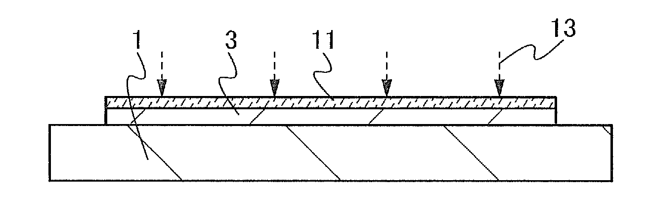
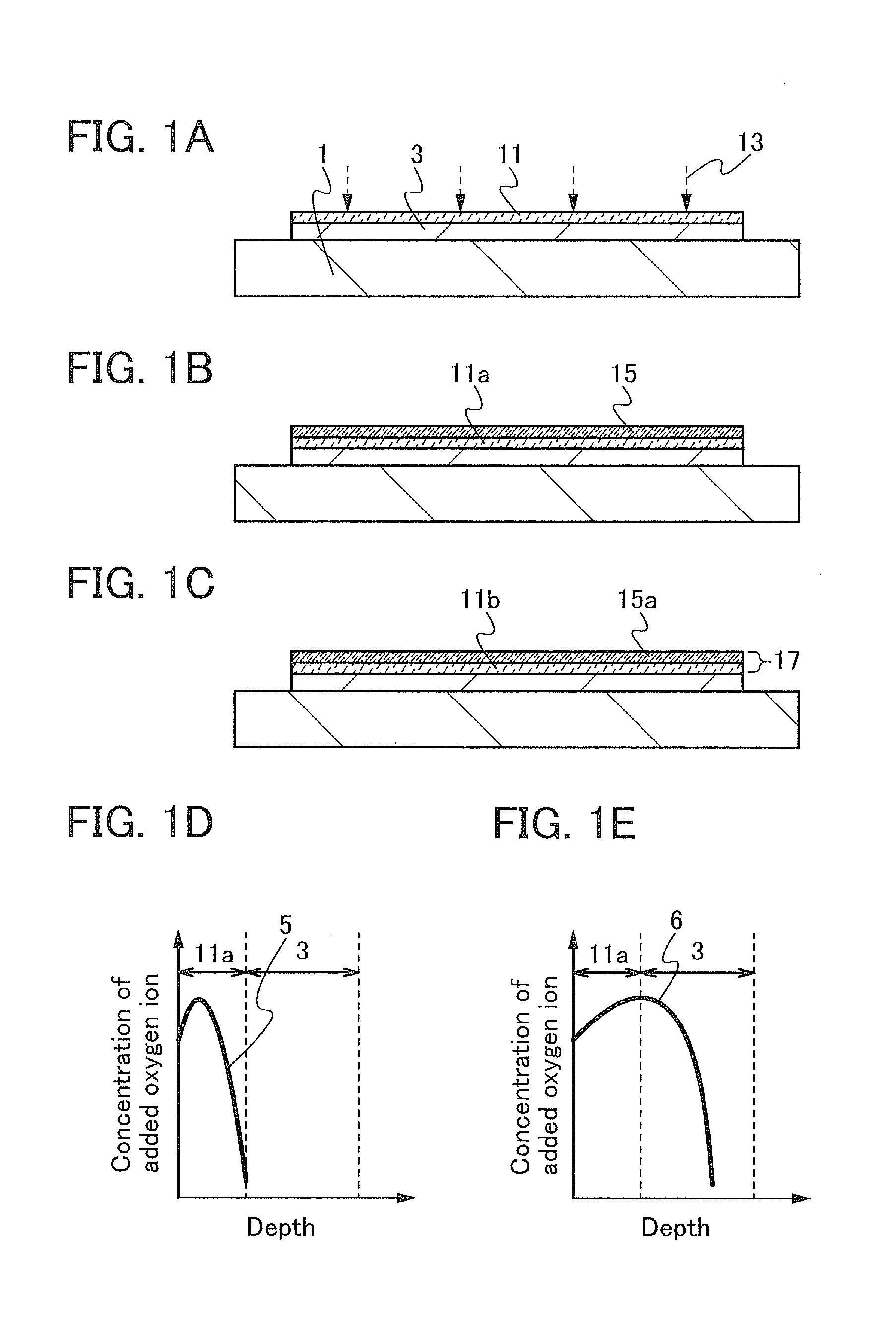
[0054]In this embodiment, a method for reducing the amount of oxygen vacancies in an oxide semiconductor film will be described. In addition, a method for forming a multilayer film including an oxide semiconductor film with a reduced density of localized levels will be described.
[0055]As illustrated in FIG. 1A, over a substrate 1, an oxide insulating film 3 functioning as a base insulating film is formed. Next, over the oxide insulating film 3 functioning as a base insulating film, an oxide film 11 containing In or Ga is formed. After that, oxygen 13 is added to the oxide film 11 containing In or Ga, so that an oxide film containing In or Ga to which oxygen is added (hereinafter, referred to as an oxide film 11a to which oxygen is added) is formed as illustrated in FIG. 1B.
[0056]The oxygen 13 that is added to the oxide film 11 containing In or Ga includes at least one of an oxygen radical, an oxygen atom, an oxygen ion, and the like. As a method for adding the oxygen 13 to the oxide...
embodiment 2
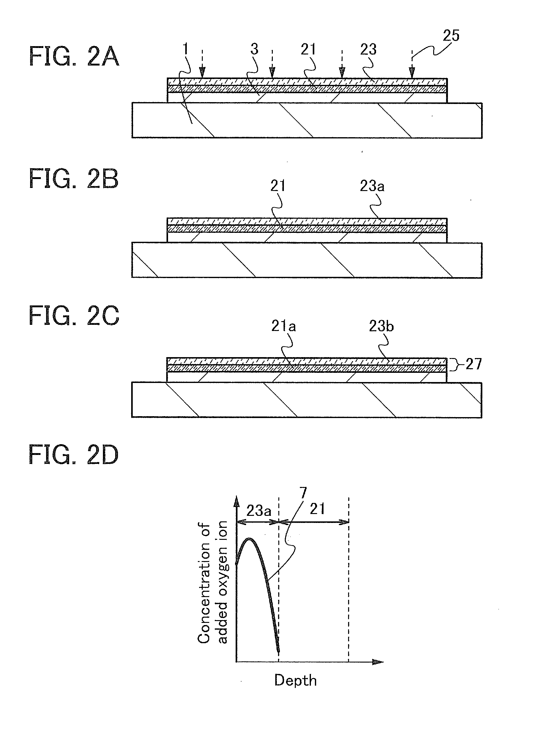
[0098]In this embodiment, a method for reducing the amount of oxygen vacancies in an oxide semiconductor film, which is different from the method in Embodiment 1, will be described. In addition, a method for forming a multilayer film including an oxide semiconductor film with a reduced density of localized levels will be described. A difference of the method in this embodiment from Embodiment 1 is that an oxide film containing In or Ga, from which oxygen is supplied to the oxide semiconductor film, is formed after the oxide semiconductor film is formed.
[0099]As illustrated in FIG. 2A, the oxide insulating film 3 functioning as a base insulating film is formed over the substrate 1. Next, an oxide semiconductor film 21 is formed over the oxide insulating film 3. Then, an oxide film 23 containing In or Ga is formed over the oxide semiconductor film 21. Then, oxygen 25 is added to the oxide film 23 containing In or Ga, so that an oxide film containing In or Ga to which oxygen is added (...
embodiment 3
[0111]In this embodiment, a method for reducing the amount of oxygen vacancies in an oxide semiconductor film, which is different from the methods in Embodiment 1 and Embodiment 2, will be described. In addition, a method for forming a multilayer film including an oxide semiconductor film with a reduced density of localized levels will be described. A difference of the method in this embodiment from Embodiment 1 is that heat treatment is performed after an oxide film containing In or Ga is formed over an oxide semiconductor film that has been formed. In addition, a difference from Embodiment 2 is that an oxide semiconductor film is formed after oxygen is added to an oxide film containing In or Ga, which has been formed over an oxide insulating film functioning as a base insulating film.
[0112]As illustrated in FIG. 3A, the oxide insulating film 3 functioning as a base insulating film is formed over the substrate 1, which is similar to that of Embodiment 1. Next, an oxide film 31 cont...
PUM
 Abstract
Description
Claims
Application Information