Detection circuit

a detection circuit and circuit technology, applied in the field of detection circuits, to achieve the effect of reliably determining peak values

Active Publication Date: 2014-05-22
MURATA MFG CO LTD
View PDF2 Cites 43 Cited by
  • Summary
  • Abstract
  • Description
  • Claims
  • Application Information

AI Technical Summary

Benefits of technology

[0010]According to the present invention, a configuration is adopted where one end side of the first high impedance circuit whose other end side is connected to the reference measurement electric potential is connected between the input terminal of the first amplification unit and the first detection electrode and one end side of the second high impedance circuit whose other end side is connected to the reference measurement electric potential is connected between the input terminal of the second amplification unit and the second detection electrode. Therefore, impedances when the input terminal sides of the first and second amplification units are individually viewed from the first and second detection electrodes become high impedances. Accordingly, since it is difficult for a detection signal to leak into the high impedance circuit, it is possible to detect even a weak detection signal. In addition, since the reference potentials of the input terminals of the first and second amplification units are fixed to a given electric potential, the fluctuations of the central potentials of the first and second detection signals become small. Accordingly, an SN ratio (Signal to Noise Ratio) is improved, and it is possible to stably detect the detection signal.
[0011]In addition, a configuration is adopted where the output terminal of the first amplification unit and the first input terminal of the differential circuit are connected to each other through the first coupling capacitor and the output terminal of the second amplification unit and the second input terminal of the differential circuit are connected to each other through the second coupling capacitor. Accordingly, owing to the first coupling capacitor, a direct-current voltage component is removed from the first output signal amplified by the first amplification unit. In addition, owing to the second coupling capacitor, a direct-current voltage component is removed from the second output signal amplified by the second amplification unit. After that, differential arithmetic processing is performed on the output signals from which the direct-current voltage components have been removed. Therefore, even if the amplification factors of the first and second amplification units are set high and the direct-current voltage components superimposed on the first and second detection signals are amplified, it is possible to remove the direct-current voltage components owing to the first and second coupling capacitors. Therefore, a signal waveform is not clamped, and distortion does not occur. As a result, a common-mode-noise cancelling performance is enhanced, and it is possible to obtain a differentially amplified signal that is desired for detection and correct.
[0013]According to the present invention, since the amplification factors of the first and second amplification units are set high so that, within the range of a driving voltage causing the operational amplifier in the differential circuit to operate, the first and second output signals become values near to a maximum value of the driving voltage, and the amplification factor of the differential circuit is set relatively low with respect to the amplification factors of the first and second amplification units, it is possible to improve the SN ratio of the detection circuit.
[0015]According to the present invention, since the amplification factors of the first and second amplification units are set high so that, within a range lower than the input level of the A / D converter circuit, the output signals of the detection circuit become values near to the input level, and the amplification factor of the differential circuit is set relatively low with respect to the amplification factors of the first and second amplification units, it is possible to improve the SN ratio of the detection circuit. In addition, it is possible to improve the degree of accuracy when an analog signal is quantized and discretized into a digital signal by the A / D converter circuit.
[0022]According to the present invention, a configuration is adopted where the digital processing circuit includes the sequential change means configured to sequentially change the determination time in response to a time interval between the peak values. Therefore, for example, even if the differential signal is detected where the period of the peak value fluctuates as the rhythmic period of the beat of a living body, which sequentially fluctuates, it is possible to prevent the determination time from extending over a plurality of periods, by sequentially changing the determination time in response to the fluctuation of the period, and it is possible to reliably determine the peak value.

Problems solved by technology

Accordingly, since it is difficult for a detection signal to leak into the high impedance circuit, it is possible to detect even a weak detection signal.

Method used


Image

  • Detection circuit
  • Detection circuit
  • Detection circuit

Examples


first embodiment

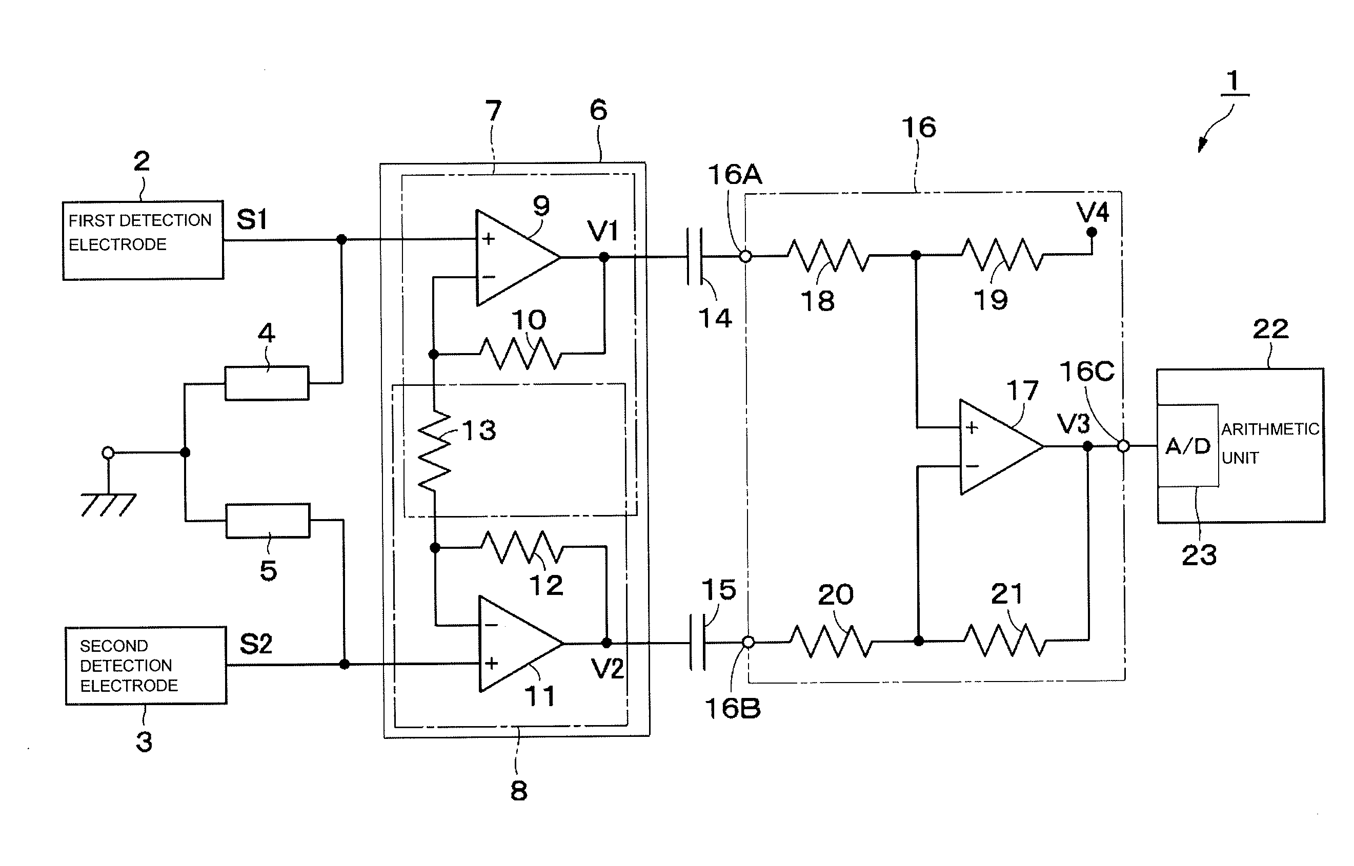
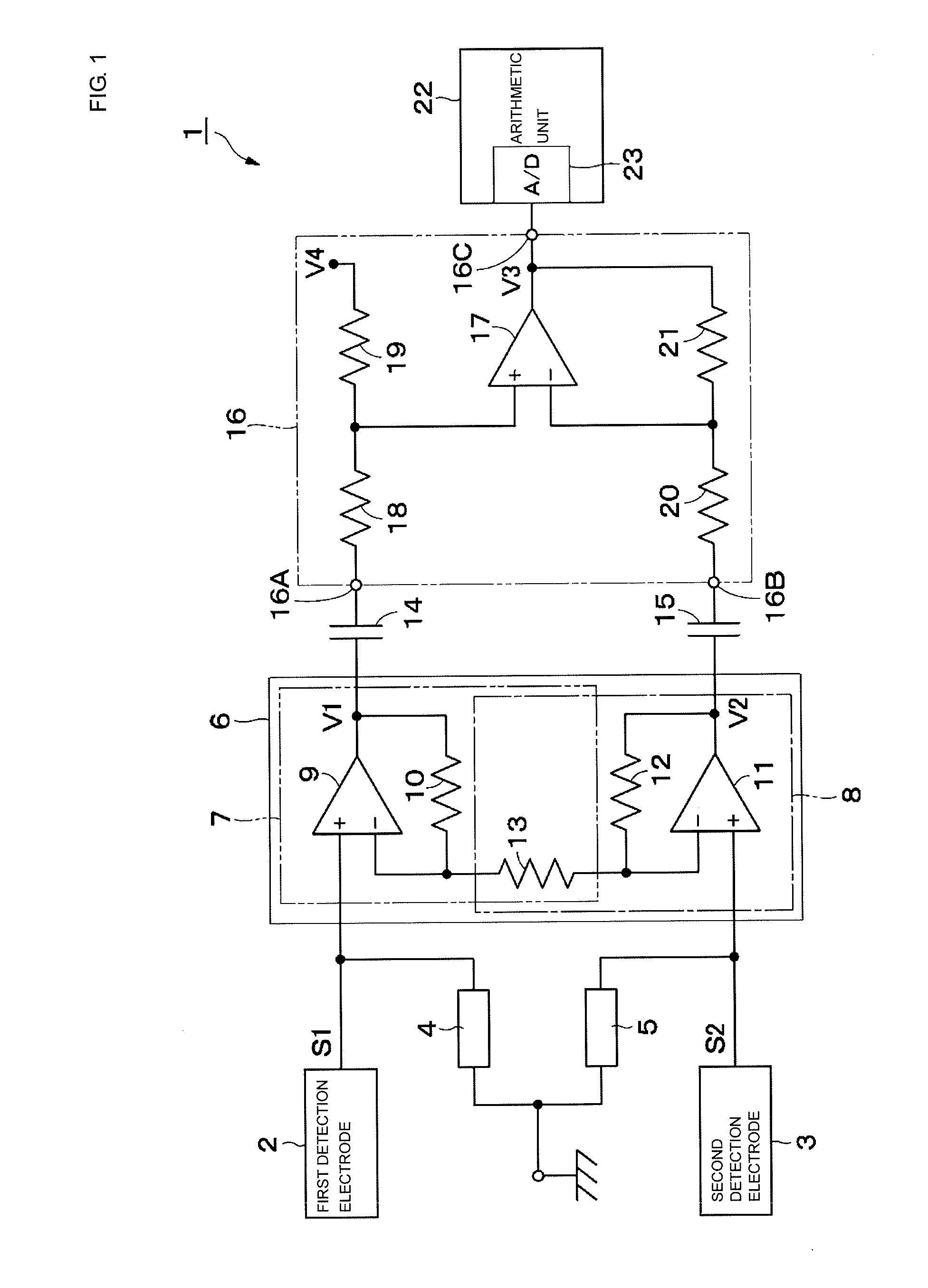
[0034]the present invention is illustrated in FIG. 1. A measurement device 1 includes first and second detection electrodes 2 and 3, first and second high impedance circuits 4 and 5, an amplifier circuit 6, first and second coupling capacitors 14 and 15, a differential amplifier circuit 16, and an arithmetic unit 22.

[0035]The first and second detection electrodes 2 and 3 are formed using, for example, a conductive film including a conductive metal material or a conductive resin material. The first and second detection electrodes 2 and 3 are attached in a state of being in direct contact with the different body surfaces of the person to be measured. The first detection electrode 2 detects a first detection signal S1 serving as an analog signal, from a first body surface. In addition, the second detection electrode 3 detects a second detection signal S2 serving as an analog signal, from a second body surface.

[0036]The first high impedance circuit 4 is configured using, for example, a ...

second embodiment

[0067]In addition, while, in the second embodiment, a configuration is adopted where the amplification factors of the first and second amplification units 33 and 34 are controlled by the single AGC circuit 38, AGC circuits may also be provided that control the first and second amplification units 33 and 34 separately.

[0068]Next, a third embodiment of the present invention will be illustrated in FIG. 4. The third embodiment is characterized by a configuration where the resistance value of a single variable resistor is adjusted by an automatic gain control circuit and the amplification factors of first and second amplification units are simultaneously controlled. In addition, in the present embodiment, the same symbol will be assigned to the same configuration element as in the above-mentioned first embodiment, and the description thereof will be omitted.

[0069]In substantially the same way as the measurement device 1 according to the first embodiment, a measurement device 41 includes ...

third embodiment

[0082]An amplifier circuit 52 is configured in substantially the same way as the amplifier circuit 42 and includes a first amplification unit 53 including the operational amplifier 9 and so forth and a second amplification unit 54 including the operational amplifier 11 and so forth. In addition, the inverting terminals of the operational amplifier 9 and the operational amplifier 11 are connected to each other through a variable resistance element 55. Furthermore, the output terminal of the first amplification unit 53 is connected to the first input terminal 16A of the differential amplifier circuit 16 through the first coupling capacitor 14, and the output terminal of the second amplification unit 54 is connected to the second input terminal 16B of the differential amplifier circuit 16 through the second coupling capacitor 15.

[0083]In addition, the first amplification unit 53 configures a non-inverting amplifier circuit using the operational amplifier 9, the resistor 10, and the va...


PUM


Abstract

An amplifier circuit includes first and second amplification units. A first detection electrode and a high impedance circuit are connected to the input terminal of the first amplification unit. A second detection electrode and a high impedance circuit are connected to the input terminal of the second amplification unit. The output terminals of the first and second amplification units output first and second output signals, and are connected to the input terminals of a differential amplifier circuit through coupling capacitors, respectively. The differential amplifier circuit operates a difference between the first and second output signals in a state where a direct-current component is omitted.

Description

CROSS REFERENCE TO RELATED APPLICATIONS[0001]The present application is a continuation of International Application No. PCT / JP2011 / 073394 filed Oct. 12, 2011, which claims priority to Japanese Patent Application No. 2010-240665, filed Oct. 27, 2010, and to Japanese Patent Application No. 2011-112520, filed on May 19, 2011, the entire contents of each of which are incorporated herein by reference.FIELD OF THE INVENTION[0002]The present invention relates to a detection circuit subjecting a weak detection signal to differential arithmetic processing, for example, a detection circuit suitable for generating biological information such as an electrocardiogram on the basis of a detection signal (the electromotive force of a heart) serving as a weak voltage waveform appearing, owing to the electrical activity of the heart, in the body surface of a person to be measured.BACKGROUND OF THE INVENTION[0003]There has been known a measurement device that detects detection signals in body surfaces...

Claims


Application Information

Patent Timeline
Patent Type & Authority Applications(United States)
IPC IPC(8): A61B5/0428A61B5/04A61B5/00A61B5/0408A61B5/308
CPCH03F3/45475H03F2200/261H03F2200/411H03F2203/45522H03F2203/45528H03G1/0035H03G3/30A61B5/302A61B5/25A61B5/316A61B5/7246
Inventor TAKAHASHI, EIJIOKUDA, NORIAKI
Owner MURATA MFG CO LTD
Why Eureka
Try Eureka