Method of reducing tungsten film roughness and resistivity

a technology of tungsten film and resistivity, applied in the field of methods, can solve the problems of increasing film roughness, increasing processing capacity, and much effort in the art to improve the morphology of tungsten film, and achieves the effects of low roughness, low resistance, and control of both resistivity and roughness of bulk deposited tungsten

Inactive Publication Date: 2014-05-29
APPLIED MATERIALS INC
View PDF7 Cites 14 Cited by
  • Summary
  • Abstract
  • Description
  • Claims
  • Application Information

AI Technical Summary

Benefits of technology

[0008]Embodiments of the present invention generally provide methods of CVD deposition of metals to maintain both low resistivity and low roughness. Specifically, the present invention generally provides methods to control both resistivity and roughness of bulk deposited tungsten. In one embodiment, a method for depositing a bulk metal can include positioning a substrate in a processing chamber, the substrate having an barrier layer formed on the surface, forming a nucleation layer, treating the nucleation layer with one or more treatment gas cycles, heating the substrate to a deposition temperature, and depositing a bulk metal layer on the nucleation layer with one or more metal layer deposition cycles. The treatment gas cycles can include flowing an activating gas, and flowing a treatment purging gas. The metal layer deposition cycles can include depositing a first layer on the nucleation layer by reacting a first processing gas, the first processing gas comprising a tungsten halide, a hydrogen-containing gas and a nitrogen-containing gas; purging the first processing gas from the chamber using a first purge gas, the first purge gas comprising the hydrogen-containing gas; depositing a second layer on the first layer by reacting a second processing gas, the second processing gas comprising the tungsten halide and the hydrogen-containing gas; and purging the second processing gas from the chamber using a second purge gas, the second purge gas comprising the hydrogen-containing gas.

Problems solved by technology

The shrinking dimensions of circuits and devices have placed additional demands on processing capabilities.
However, increased grain size results in increased film roughness.
Therefore, there is much effort in the art to improve the tungsten film morphology while maintaining the low film resistivity.

Method used


Image

  • Method of reducing tungsten film roughness and resistivity
  • Method of reducing tungsten film roughness and resistivity
  • Method of reducing tungsten film roughness and resistivity

Examples


Embodiment Construction

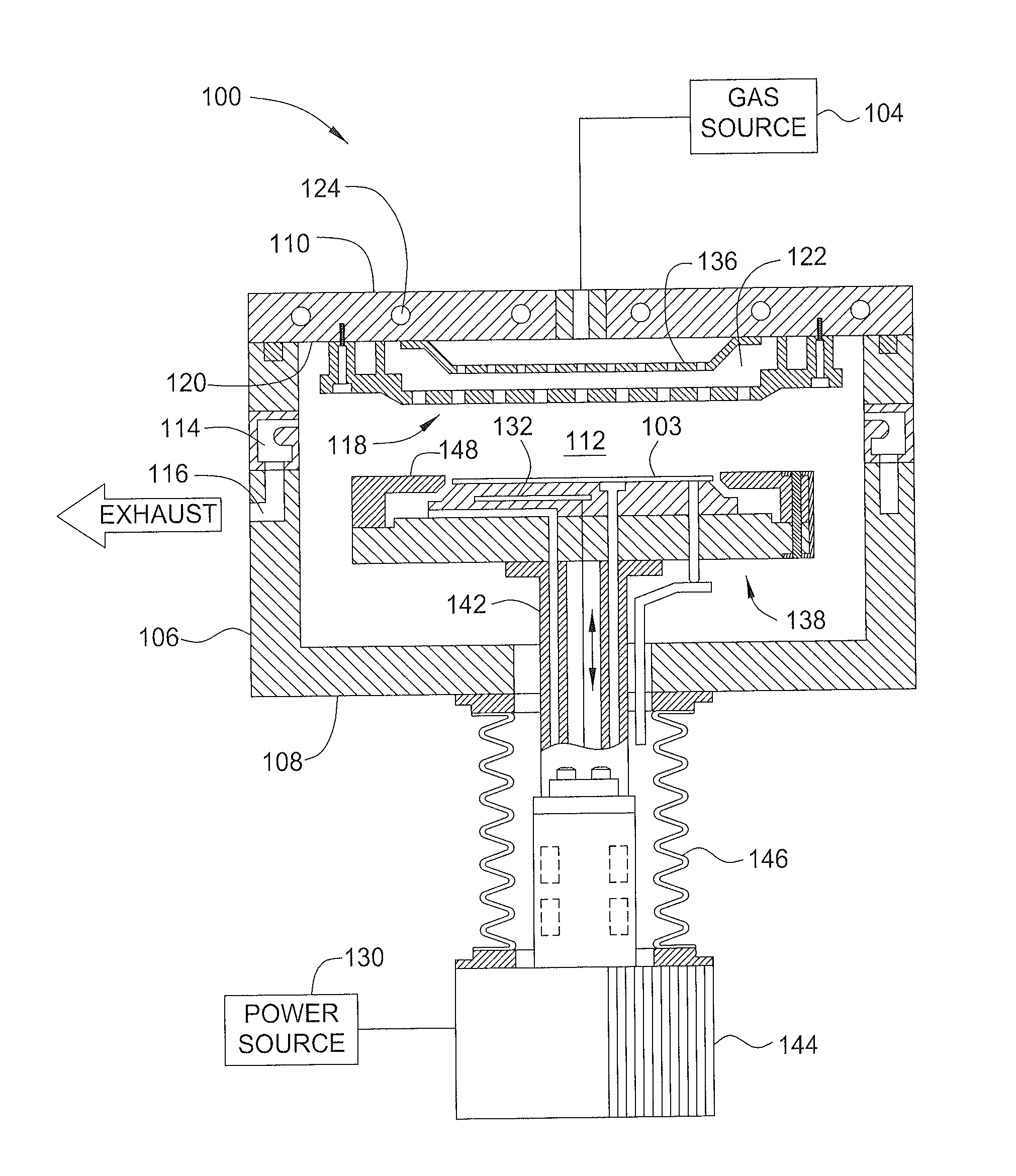
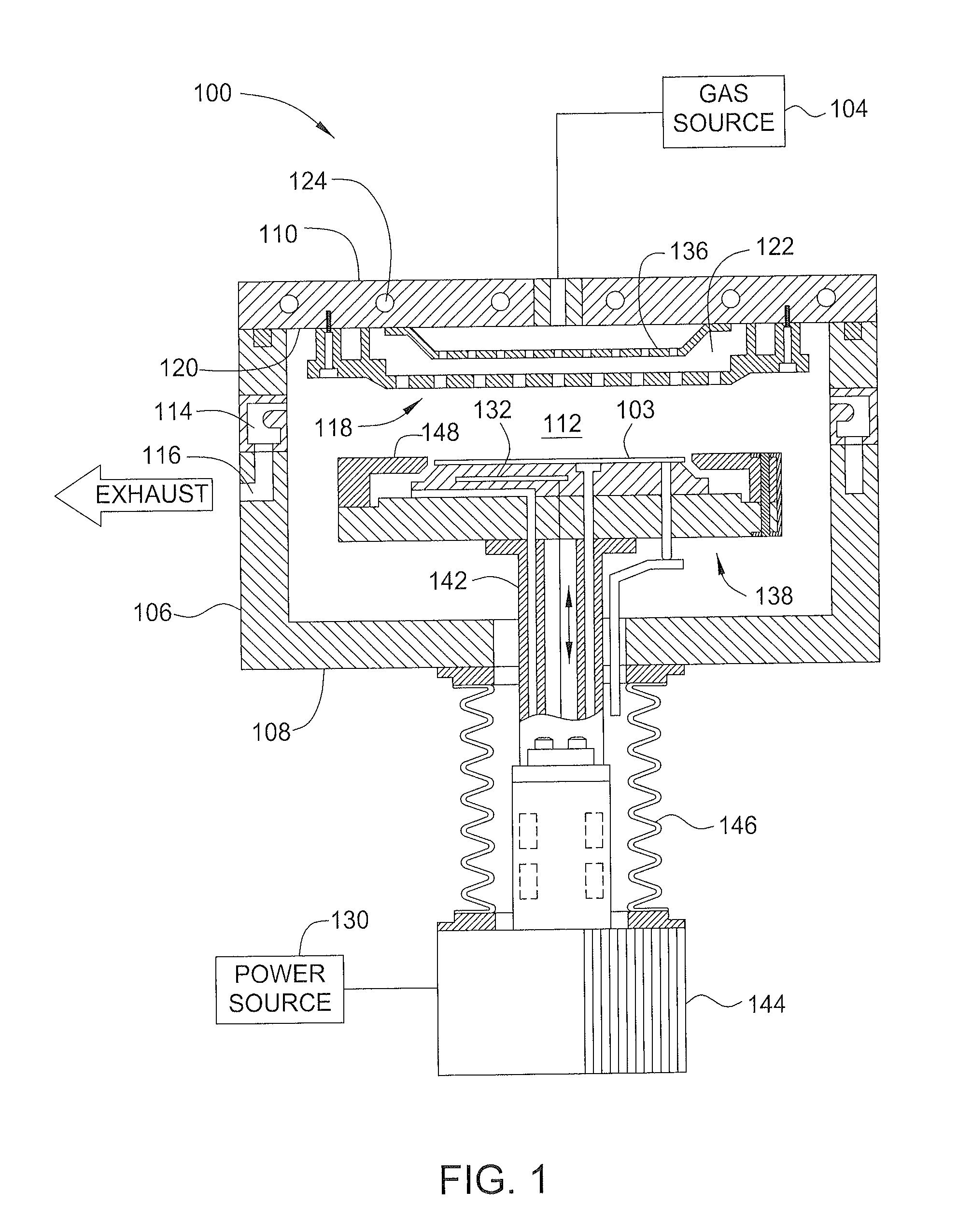
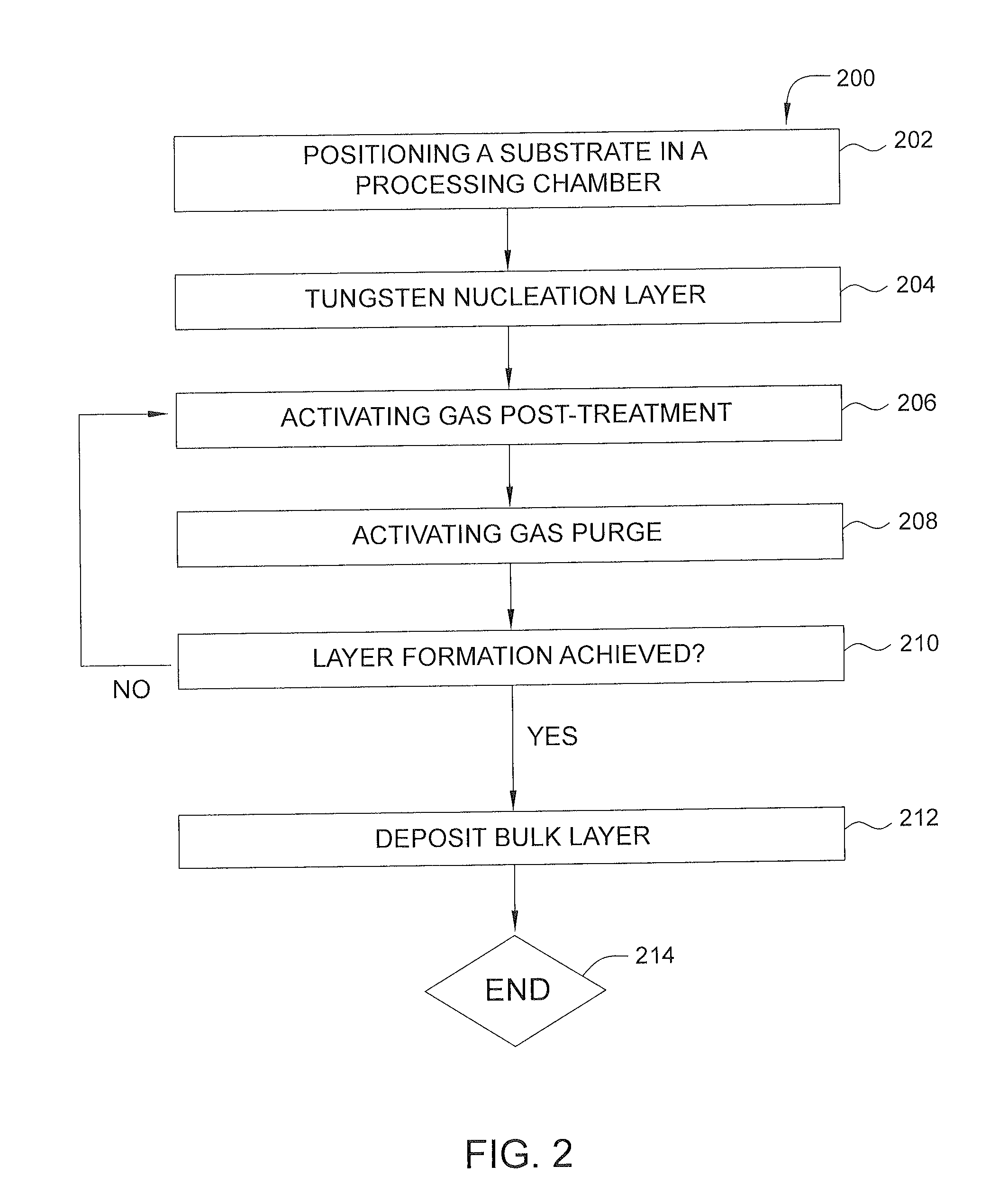
[0015]Embodiments of the present invention generally provide methods of CVD deposition of metals, such as tungsten, with a smaller grain size while maintaining a low resistivity. Deposition of tungsten in features by standard techniques can lead to an increase in both the starting bulk and the overall resistance of the deposition product. Standard CVD bulk tungsten deposition can create a low resistivity film, such as a tungsten film from WF6 and H2 which has a resistivity of less than 20 μΩ-cm. However, these low resistivity films have a high roughness due to the formation of large crystals. Other tungsten containing layers, such as tungsten nitride (WN) have a lower roughness but at a cost of increased resitivity. The methods described herein reduce the crystal size of the formed tungsten layer while maintaining low resistivity.

[0016]Though exemplary embodiments and explanations focus on tungsten or titanium, it is understood that metals other than tungsten can used with the depos...


PUM

PropertyMeasurementUnit
time periodaaaaaaaaaa
diameteraaaaaaaaaa
diameteraaaaaaaaaa

Abstract

Methods for controlling crystal size in bulk tungsten layers are disclosed herein. Methods for depositing a bulk tungsten metal layer can include positioning a substrate with a barrier layer in a processing chamber, forming a tungsten nucleation layer, post-treating the nucleation layer with one or more treatment gas cycles including an activating gas and a purging gas, heating the substrate to a deposition temperature, and depositing a bulk tungsten layer with alternating nitrogen flow on the nucleation layer. The post-treatment cycling can be applied optionally to the bulk metal deposition with alternating nitrogen flow.

Description

CROSS-REFERENCE TO RELATED APPLICATIONS[0001]This application claims benefit of U.S. Provisional Patent Application Ser. No. 61 / 729,925 (APPM / 16530L), filed Nov. 26, 2012, which is herein incorporated by reference.BACKGROUND OF THE INVENTION[0002]1. Field of the Invention[0003]Embodiments of the invention relate generally to methods for processing a substrate during semiconductor manufacturing. Specifically, embodiments of the invention relate to methods of treating a nucleation layer prior to a CVD deposition process.[0004]2. Description of the Related Art[0005]Reliably producing nanometer-sized features is one of the key technologies for the next generation of semiconductor devices. The shrinking dimensions of circuits and devices have placed additional demands on processing capabilities. The multilevel interconnects that lie at the heart of integrated circuit technology require precise processing of high aspect ratio features, such as vias and other interconnects. Reliable format...

Claims


Application Information

Patent Timeline
Patent Type & Authority Applications(United States)
IPC IPC(8): C23C16/06
CPCC23C16/06C23C16/0281C23C16/14C23C16/45525
Inventor KHANDELWAL, AMITGELATOS, AVGERINOS V.
Owner APPLIED MATERIALS INC
Why Eureka
Try Eureka