Nanomesh complementary metal-oxide-semiconductor field effect transistors

a complementary metal-oxidesemiconductor and field effect transistor technology, applied in the field of semiconductor structure, can solve the problems of reducing the threshold voltage of an nfet and being particularly difficult to adjust the threshold voltag

Inactive Publication Date: 2014-06-05
GLOBALFOUNDRIES INC
View PDF3 Cites 180 Cited by
  • Summary
  • Abstract
  • Description
  • Claims
  • Application Information

AI Technical Summary

Problems solved by technology

However, such a change in the valence band offset in the silicon-germanium alloy degrades the threshold voltage of an NFET.
Further, for undoped body fully depleted field effect transistors, threshold voltage adjustment is particularly challenging because doping cannot be used to tune the threshold voltage.

Method used


Image

  • Nanomesh complementary metal-oxide-semiconductor field effect transistors
  • Nanomesh complementary metal-oxide-semiconductor field effect transistors
  • Nanomesh complementary metal-oxide-semiconductor field effect transistors

Examples


Embodiment Construction

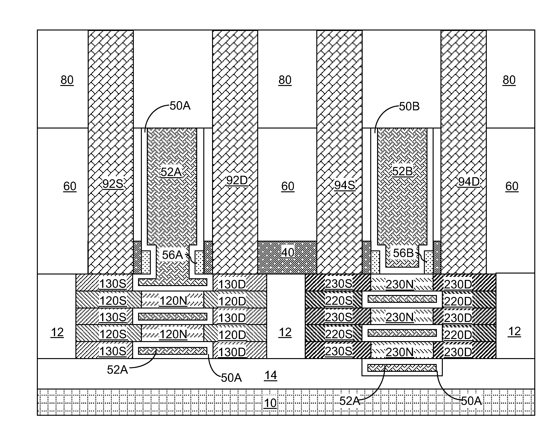
[0057]As stated above, the present disclosure relates to nanomesh complementary metal-oxide-semiconductor field effect transistors (MOSFET's) and a method of manufacturing the same. Aspects of the present disclosure are now described in detail with accompanying figures. It is noted that like reference numerals refer to like elements across different embodiments. The drawings are not necessarily drawn to scale.

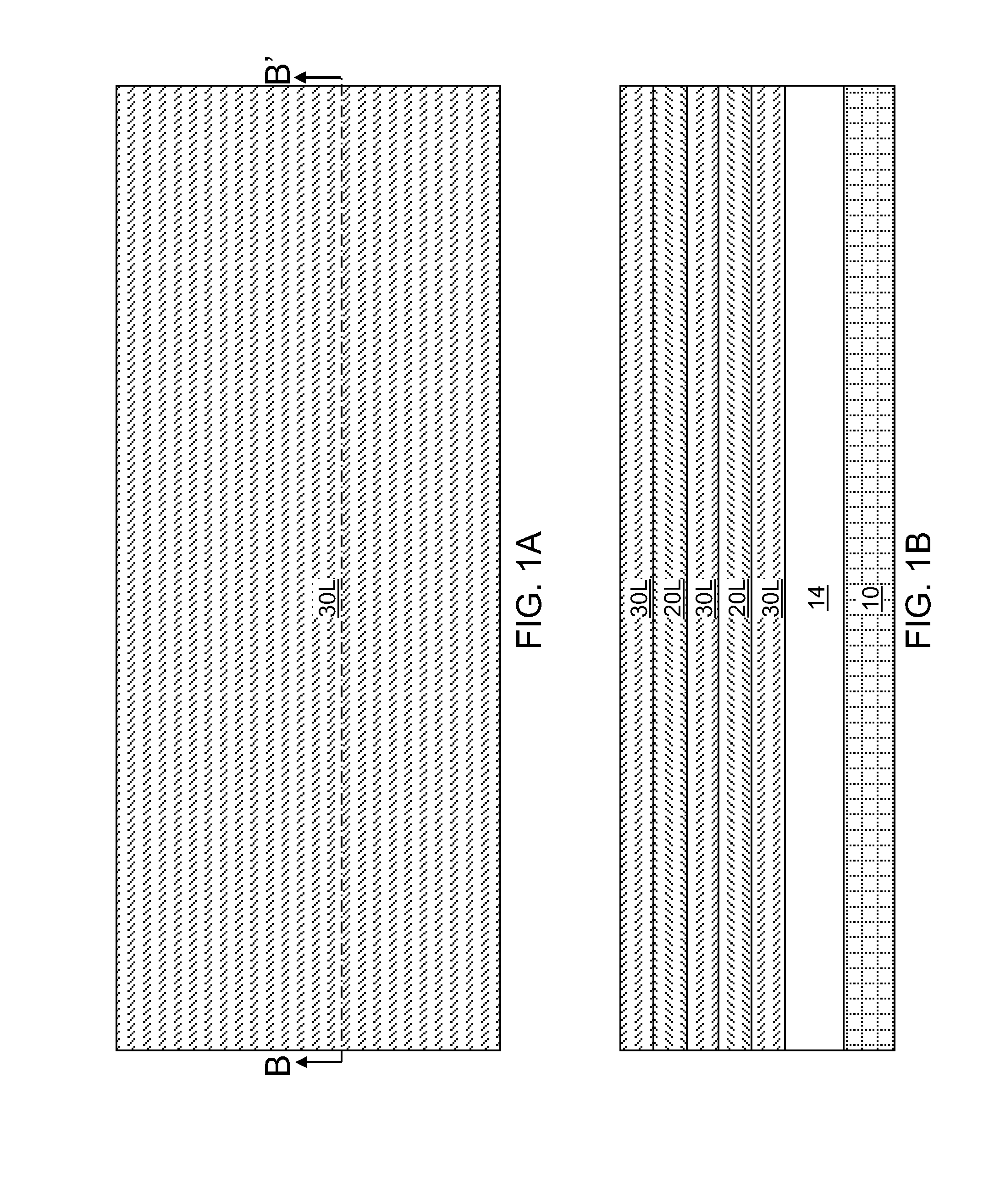
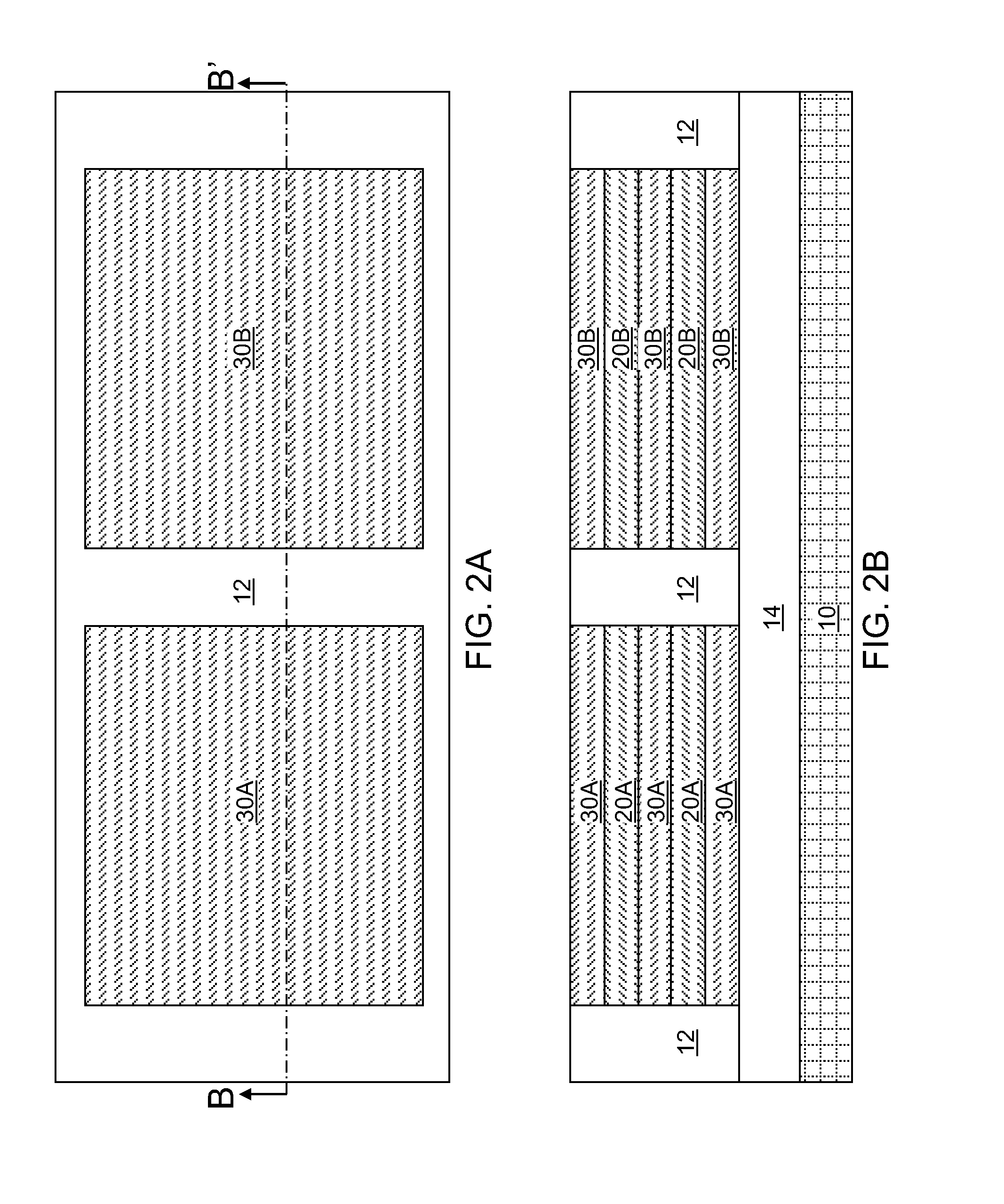
[0058]Referring to FIGS. 1A and 1B, an exemplary semiconductor structure according to an embodiment of the present disclosure includes a handle substrate 10, an insulator layer 14, and an alternating stack of a silicon-germanium alloy and a germanium-free silicon material. The handle substrate 10 can include a semiconductor material, an insulator material, a conductive material, or a combination thereof. The thickness of the handle substrate 10 can be from 50 microns to 2 mm, although lesser and greater thicknesses can also be employed. The handle substrate 14 provides mechanic...


PUM


Abstract

An alternating stack of first and second semiconductor layers is formed. Fin-defining mask structures are formed over the alternating stack. A planarization dielectric layer and first and second gate cavities therein are subsequently formed. The first and second gate cavities are extended downward by etching the alternating stack employing a combination of the planarization layer and the fin-defining mask structures as an etch mask. The germanium-free silicon material is isotropically etched to laterally expand the first gate cavity and to form a first array of semiconductor nanowires including the silicon-germanium alloy, and the silicon-germanium alloy is isotropically etched to laterally expand the second gate cavity and to form a second array of semiconductor nanowires including the germanium-free silicon material. The first and second gate cavities are filled with replacement gate structures. Each replacement gate structure laterally can surround a two-dimensional array of semiconductor nanowires.

Description

RELATED APPLICATIONS[0001]The present application is related to co-assigned and co-pending U.S. application Ser. No. ______ (Attorney Docket No: YOR920120646US1; SSMP 29103), which is incorporated herein by reference.BACKGROUND[0002]The present disclosure relates to a semiconductor structure, and particularly to nanomesh complementary metal-oxide-semiconductor field effect transistors (MOSFET's) and a method of manufacturing the same.[0003]A silicon-germanium alloy channel is desirable for a p-type field effect transistor (PFET) and a silicon channel is desirable for an n-type field effect transistor (NFET). Particularly, a silicon-germanium alloy channel can provide enhance mobility and a valance band offset from the band gap structure of silicon. Thus, a PFET employing the silicon-germanium alloy channel can provide a lower threshold voltage than a PFET employing a silicon channel. However, such a change in the valence band offset in the silicon-germanium alloy degrades the thresh...

Claims


Application Information

Patent Timeline
Patent Type & Authority Applications(United States)
IPC IPC(8): H01L27/12H01L21/84
CPCH01L21/845H01L27/1211B82Y10/00H01L21/84H01L27/1203H01L29/0673H01L29/42372H01L29/42392H01L29/66439H01L29/775H01L29/78696
Inventor CHANG, JOSEPHINE B.CHANG, PAULGUILLORN, MICHAEL A.SLEIGHT, JEFFREY W.
Owner GLOBALFOUNDRIES INC
Why Eureka
Try Eureka