

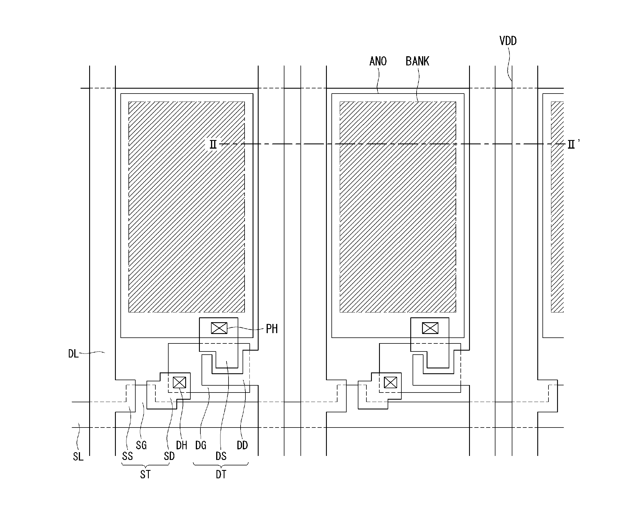
Large Area Organic Light Emitting Diode Display and Method for Manufacturing the Same
a technology of organic light emitting diodes and large area, which is applied in the direction of thermoelectric device junction materials, electrical equipment, and semiconductor devices. it can solve the problems of difficult to pattern organic light emitting materials using the current photo lithography method, and it is almost impossible to form organic light emitting layers over a large area using the screen mask process, and achieves high resolution and reliable and stable production yield.
- Summary
- Abstract
- Description
- Claims
- Application Information
AI Technical Summary
Benefits of technology
Problems solved by technology
Method used
Image

Examples
second embodiment
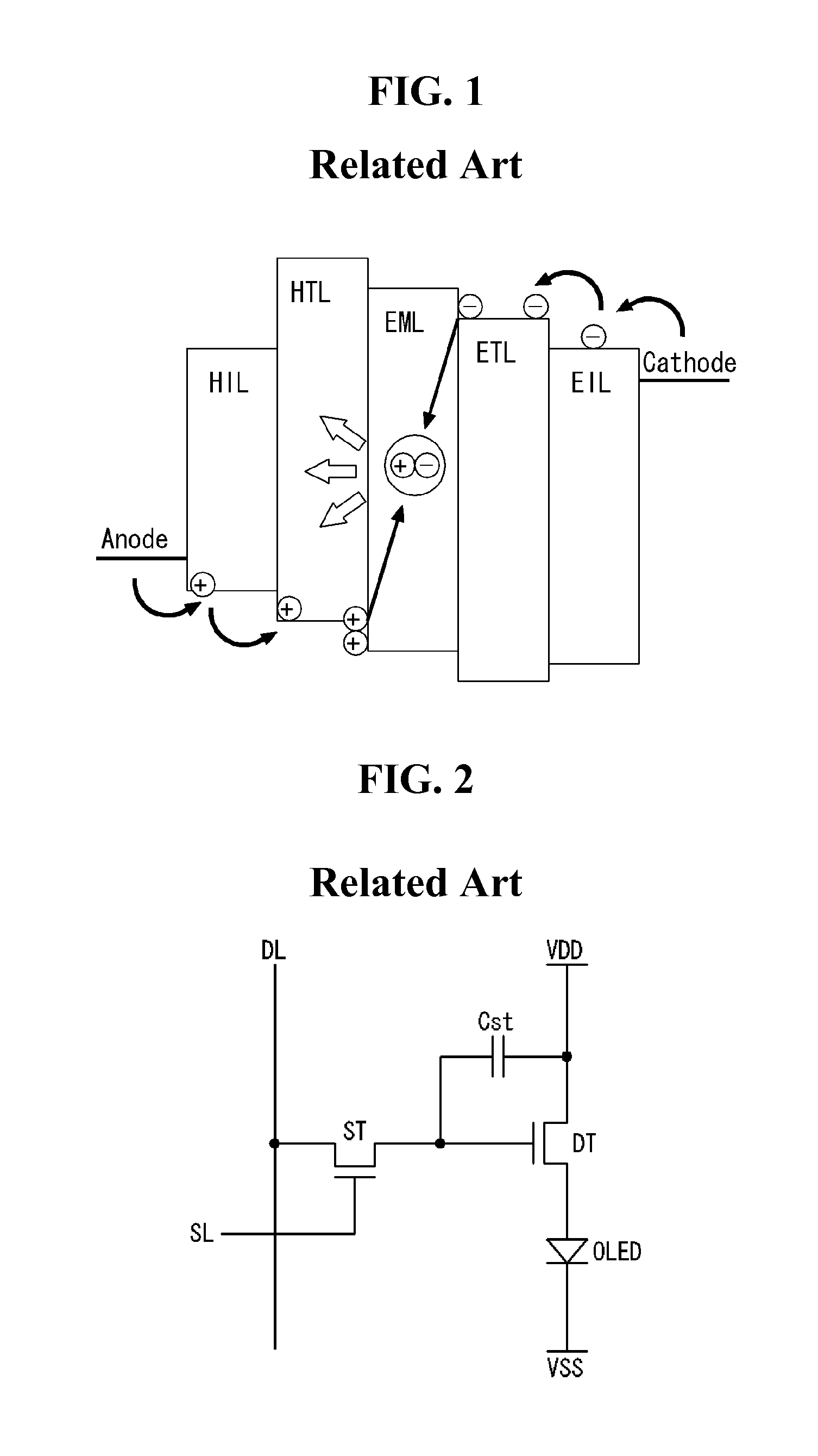
[0070]Referring to FIG. 8, we will explain a large area organic light emitting diode display according to the present disclosure. A hole injection layer HIL is deposited on the anode electrode ANO and the bank BANK, over the whole surface of the substrate SUB. A hole transport layer HTL is deposited on the hole injection layer HIL over the whole surface of the substrate SUB. As the hole injection layer HIL and the hole transport layer HTL cover the whole surface of the substrate SUB, a photo mask process or screen mask process is not required.
[0071]In each pixel area, any one of the red organic emission layer REML, the green organic emission layer GEML and the blue organic emission layer BEML is formed between the banks BANK on the hole transport layer HTL. Actually, the organic emission layers REML, GEML and BEML define their respective emitting areas. Therefore, it is preferred for the organic light emitting layers to cover the emitting area between adjacent banks BANK.
[0072]Furth...
third embodiment
[0074]Now, referring to FIG. 9, we will explain a large area organic light emitting diode display according to the present disclosure. A hole injection layer HIL is deposited on the anode electrode ANO and the bank BANK, and covers the whole surface of the substrate SUB. On the hole injection layer HIL, a hole transport layer HTL is deposited covering the whole surface of the substrate SUB. As the hole injection layer HIL and the hole transport layer HTL cover the whole surface of the substrate SUB, a photo mask process or screen mask process is not required.
[0075]In each pixel area, any one of the red organic emission layer REML, the green organic emission layer GEML and the blue organic emission layer BEML is formed between the banks BANK on the hole transport layer HTL. Additionally, the emitting area is defined by the organic emission layers REML, GEML and BEML. Therefore, it is preferable for the organic light emitting layers to cover the emitting area between adjacent banks BA...
PUM
 Abstract
Description
Claims
Application Information