

Semiconductor device
a technology of semiconductors and semiconductors, applied in the field of semiconductor devices, can solve the problems of less suitable for high-speed operation than binary memory, increase in memory capacity, and inability to meet the needs of information storage, etc., and achieve the effect of high convenience and new structur
- Summary
- Abstract
- Description
- Claims
- Application Information
AI Technical Summary
Benefits of technology
Problems solved by technology
Method used
Image

Examples
embodiment 1
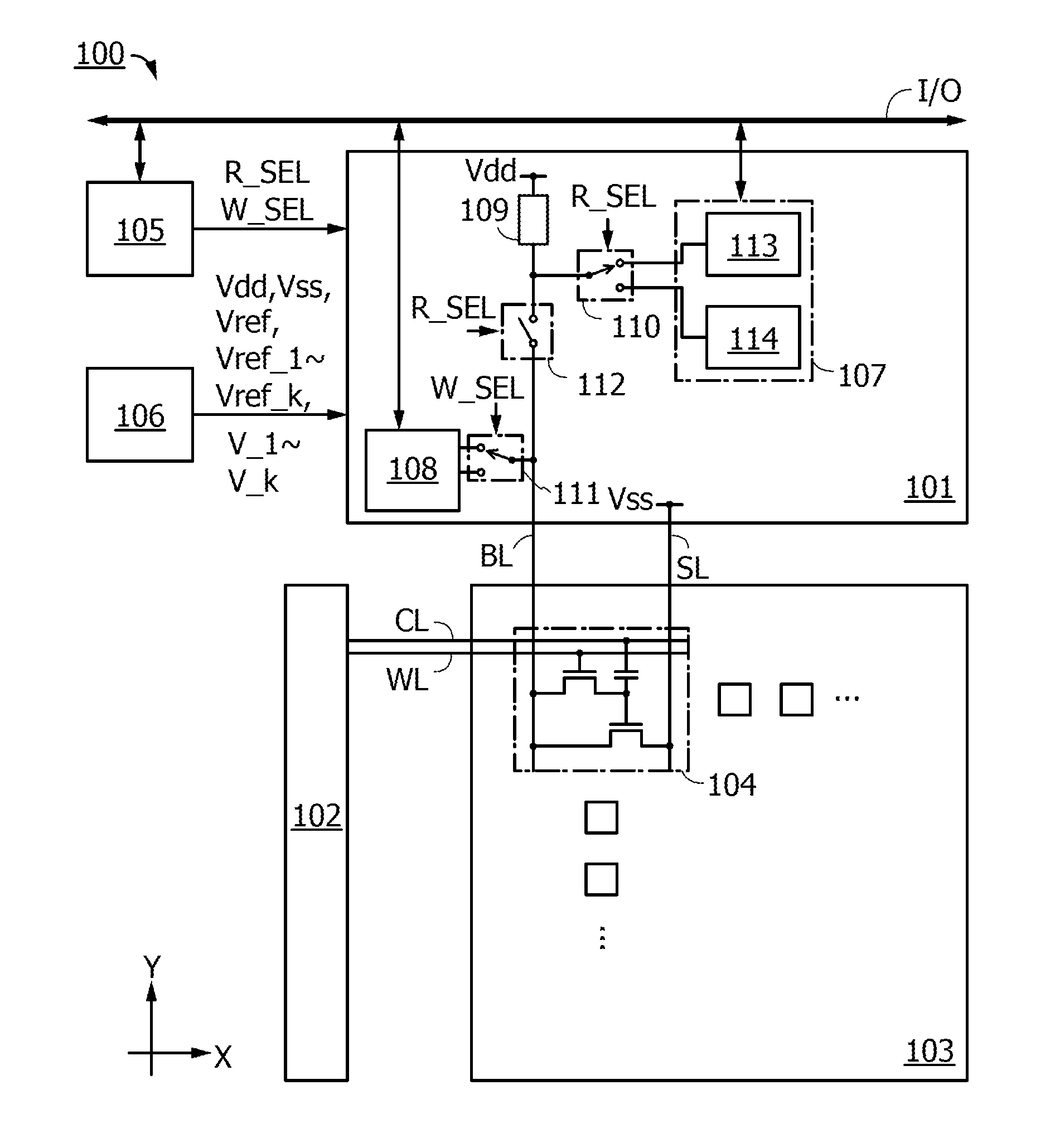
[0063]In Embodiment 1, a basic structure of a semiconductor device of one embodiment of the disclosed invention will be described with reference to FIG. 1.
[0064]FIG. 1 is a block diagram illustrating an example of a semiconductor device 100.
[0065]Note that a semiconductor device refers to a device including a semiconductor element. The semiconductor device includes a driver circuit that drives a circuit including a semiconductor element, and the like, and also includes a control circuit, a voltage generator circuit, or the like provided over a separate substrate.
[0066]The block diagram of the semiconductor device 100 in FIG. 1 shows a circuit (hereinafter referred to as driver circuit 101) for supplying a signal to a wiring provided in the Y direction, a circuit (hereinafter referred to as driver circuit 102) for supplying a signal to a wiring provided in the X direction, and a circuit (hereinafter referred to as memory circuit 103) that stores data in accordance with signals suppli...
embodiment 2
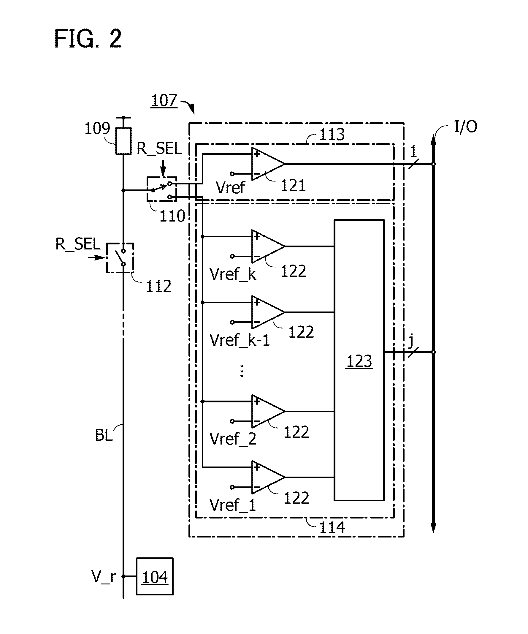
[0104]In Embodiment 2, a structure example of the reading circuit described in Embodiment 1 will be described with reference to FIG. 2.
[0105]The block diagram of the reading circuit 107 in FIG. 2 shows the reading circuit 113, the reading circuit 114, a comparator 121, comparators 122, and an arithmetic circuit 123. FIG. 2 also shows the memory cell 104, the load 109, the read switching circuit 110, the read switching switch 112, and the input / output unit I / O.
[0106]The reading circuit 113 can compare the levels of the reference voltage Vref and a read data voltage that is input to the comparator 121 in response to switching of the read switching circuit 110 and the read switching switch 112. As the determination result of the comparison by the reading circuit 113, 1-bit data having H level or L level, that is, 1-bit data of data ‘0’ or data ‘1’ is output to the input / output unit I / O.
[0107]In the reading circuit 114, a read data voltage input by switching of the read switching circui...
embodiment 3
[0112]In Embodiment 3, a structure example of the writing circuit described in Embodiment 1 will be described with reference to FIG. 3.
[0113]The block diagram of the writing circuit 108 in FIG. 3 shows a writing circuit 131 and a writing circuit 132. FIG. 3 also shows the memory cell 104, the write switching circuit 111, the voltage generator circuit 106, and the input / output unit I / O.
[0114]The writing circuit 131 is supplied with data through the input / output unit I / O and outputs a voltage corresponding to the data to the memory cell 104 through the bit line BL. For example, the writing circuit 131 is supplied with voltages V—1 and V_k serving as write data voltages for binary data from the voltage generator circuit 106, and outputs one of the voltages in accordance with the data.
[0115]The writing circuit 132 is supplied with data through the input / output unit I / O and outputs a voltage corresponding to the data to the memory cell 104 through the bit line BL. For example, the writin...
PUM
 Abstract
Description
Claims
Application Information