Parasitic inductance reduction for multilayered board layout designs with semiconductor devices

a semiconductor device and layout technology, applied in the field of circuit boards and circuit board layouts, can solve the problems of reducing the efficiency of power converters, limiting the performance of converter components on the circuit board layout, and increasing voltage overshoot, so as to achieve the effect of minimizing parasitic inductan

Active Publication Date: 2014-07-03
EFFICIENT POWER CONVERSION CORP
View PDF2 Cites 40 Cited by
  • Summary
  • Abstract
  • Description
  • Claims
  • Application Information

AI Technical Summary

Benefits of technology

[0016]The present invention provides a circuit board layout design which eliminates the above-noted disadvantages of the prior art designs. Specifically, the circuit board of the present invention comprises a top layer, a bottom layer, and at least one inner layer connected by vias to the top layer so that a high frequency power loop is formed in a path extending between the top layer and the inner layer. Advantageously, the layout design according to the present invention minimizes parasitic inductance independent of board thickness and without requiring a shield layer.

Problems solved by technology

With higher switching speeds and lower package parasitic inductance, the circuit board layout of converter components becomes a limiting factor in converter performance because the layout of components has a significant effect on the overall level of parasitic inductance.
High frequency power loop inductance, controlled by circuit board layout, is a major contributor to loss of power converter efficiency.
Another impact of the faster switching speeds provided by lower figure of merit devices is an increase in voltage overshoot when compared to devices with slower switching speeds.
The shield layer also contributes additional conductive losses to the power converter, decreasing performance.

Method used


Image

  • Parasitic inductance reduction for multilayered board layout designs with semiconductor devices
  • Parasitic inductance reduction for multilayered board layout designs with semiconductor devices
  • Parasitic inductance reduction for multilayered board layout designs with semiconductor devices

Examples


Embodiment Construction

[0037]In the following detailed description, reference is made to certain embodiments. These embodiments are described with sufficient detail to enable those skilled in the art to practice them. It is to be understood that other embodiments may be employed and that various structural, logical, and electrical changes may be made.

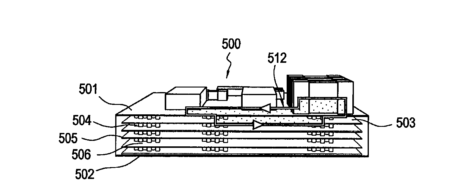
[0038]The circuit board layout designs of the present invention described below provide reduced loop size, magnetic field self-cancellation, consistent inductance independent of board thickness, and a single sided circuit board design providing high efficiency for a multi-layer structure. The circuit board layout design of the present invention utilizes the first inner layer as a power loop return path. This return path is located directly underneath the power loop of the top loop, allowing for the smallest physical loop size combined with magnetic field self-cancellation.

[0039]While embodiments described herein are described in connection with certain types ...


PUM


Abstract

A highly efficient, single sided circuit board layout design providing magnetic field self-cancellation and reduced parasitic inductance independent of board thickness. The low profile power loop extends through active and passive devices on the top layer of the circuit board, with vias connecting the power loop to a return path in an inner layer of the board. The magnetic effect of the portion of the power loop on the top layer is reduced by locating the inner layer return path directly underneath the power loop path on the top layer.

Description

BACKGROUND OF THE INVENTION[0001]1. Field of the Invention[0002]The present invention relates generally to power converters and circuits, e.g., circuit boards and, more particularly, to circuit board layouts for improving power converter performance.[0003]2. Description of the Related Art[0004]The improvement of power field effect transistor (FET) technologies such as silicon metal oxide semiconductor FETs and the introduction of gallium nitride (GaN) based transistors allow switching power supplies to achieve faster switching speeds by reducing switching related charges and package parasitic inductance. With higher switching speeds and lower package parasitic inductance, the circuit board layout of converter components becomes a limiting factor in converter performance because the layout of components has a significant effect on the overall level of parasitic inductance. An improved circuit board layout is needed to minimize the high frequency loop inductance in a multilayer circui...

Claims


Application Information

Patent Timeline
Patent Type & Authority Applications(United States)
IPC IPC(8): H01L23/522H01L27/06
CPCH01L23/5222H01L27/0629H02M7/003H01L2924/0002H01L2924/15192H01L23/49822H05K1/0231H05K1/0243H05K1/0265H05K2201/0792H05K2201/10166H01L2924/00
Inventor REUSCH, DAVIDSTRYDOM, JOHAN TJEERD
Owner EFFICIENT POWER CONVERSION CORP
Why Eureka
Try Eureka