Low Power, High Speed Multi-Channel Chip-to-Chip Interface using Dielectric Waveguide

Active Publication Date: 2014-07-03
POINT2 TECH
View PDF1 Cites 26 Cited by
  • Summary
  • Abstract
  • Description
  • Claims
  • Application Information

AI Technical Summary

Benefits of technology

[0008]At least one of both ends of the dielectric waveguide is shaped linearly to opt

Problems solved by technology

The drastic attenuation in the conventional copper wire line interconnect

Method used


Image

  • Low Power, High Speed Multi-Channel Chip-to-Chip Interface using Dielectric Waveguide
  • Low Power, High Speed Multi-Channel Chip-to-Chip Interface using Dielectric Waveguide
  • Low Power, High Speed Multi-Channel Chip-to-Chip Interface using Dielectric Waveguide

Examples


Embodiment Construction

[0028]The invention is described more fully hereinafter with reference to the accompanying drawings, in which exemplary embodiments of the invention are shown. This invention may, however, be embodied in many different forms and should not be construed as limited to the embodiments set forth herein. Rather, these exemplary embodiments are provided so that this disclosure is thorough, and will fully convey the scope of the invention to those skilled in the art. In the drawings, the size and relative sizes of layers and regions may be exaggerated for clarity. Like reference numerals in the drawings denote like elements.

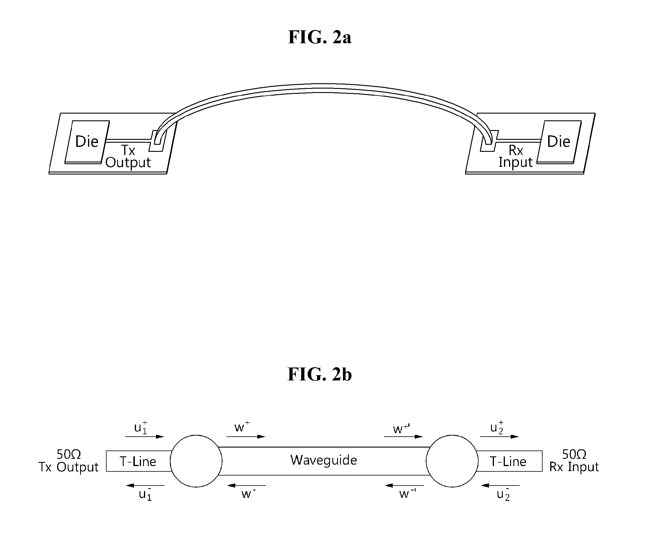
[0029]An exemplary embodiment of the present invention may provide an improved interconnect instead of electrical wire line. A novel type of dielectric waveguide named, for example, an electrical fiber may be presented to replace conventional copper line. The electrical fiber may be defined as a dielectric waveguide with metal cladding.

[0030]Dielectrics with frequency i...


PUM


Abstract

An exemplary embodiment of the present invention provides an improved dielectric waveguide named electrical fiber. The electrical fiber with a metal cladding may isolate the interference of the signals in other wireless channels and adjacent electrical fibers, which typically causes band-limitation problem, for a smaller radiation loss and better signal guiding to lower the total transceiver power consumption as the transmit distance increases. Also, the electrical fiber may have frequency independent attenuation characteristics to enable high data rate transfer with little or even without any additional receiver-side compensation due to vertical coupling of the electrical fiber and an interconnection device.

Description

CROSS-REFERENCE TO RELATED APPLICATION[0001]This application claims the priority benefit of Korean Patent Application No. 10-2012-0154094, filed on Dec. 27, 2012, and Korean Patent Application No. 10-2013-0123344, filed on Oct. 16, 2013 in the Korean Intellectual Property Office, the disclosure of which are incorporated herein by reference.BACKGROUND[0002]1. Field of the Invention[0003]Exemplary embodiments of the present invention relate to a waveguide to propagate a signal on a low power—high speed multi-channel chip-to-chip interface using a dielectric waveguide.[0004]2. Description of the Related Art[0005]Ever increasing demand for bandwidth in the wire line communications necessitates high-speed, low-power, low-cost I / O. The drastic attenuation in the conventional copper wire line interconnects caused by skin effect in high frequencies limits the system performance. Penalty in receiver power, cost and area occurs to compensate for the loss in the interconnection, and increases ...

Claims


Application Information

Patent Timeline
IPC IPC(8): H01P5/04H01P3/16
CPCH01P3/165H01P3/122H01P3/16H01P5/087H01P5/107H01P3/08
Inventor BAE, HYEON MINSONG, HA ILJIN, HUXIAN
Owner POINT2 TECH
Why Eureka
Try Eureka