Methods of patterning block copolymer layers

a copolymer layer and block technology, applied in the field of patterning a block copolymer layer, can solve the problems of difficult manufacturing of nano-patterns less than or equal to about 20 nanometers (nm), and the difficulty of conventional photolithography technology in realizing fine nano-sized patterns, so as to improve the degree of pattern alignment, minimize the effect of dewetting phenomenon and increase the pattern area

Inactive Publication Date: 2014-07-03
SAMSUNG ELECTRONICS CO LTD
View PDF3 Cites 13 Cited by
  • Summary
  • Abstract
  • Description
  • Claims
  • Application Information

AI Technical Summary

Benefits of technology

[0018]In one or more embodiment of the present invention, by controlling the edge structure of the topographic guide pattern, uniformity of a thin film in post-treatment processes may be secured. By way of an example, the dewetting phenomenon may be minimized even in a thin film having a thickness of less than or equal to about 40 nanometers (nm), and thereby an increased pattern area of the self-assembled structure of a block copolymer directed by the guide pattern is obtained. In addition, minimizing the dewetting phenomenon may improve the degree of pattern alignment, decrease the density of defects, and enable free control over the time of post-treatment processes.

Problems solved by technology

Conventional photolithography technology has difficulties in realizing a fine nano-sized pattern.
In particular, a nano-pattern of less than or equal to about 20 nanometers (nm) are difficult to manufacture, due to a wavelength resolution limit.

Method used


Image

  • Methods of patterning block copolymer layers
  • Methods of patterning block copolymer layers
  • Methods of patterning block copolymer layers

Examples


example 1

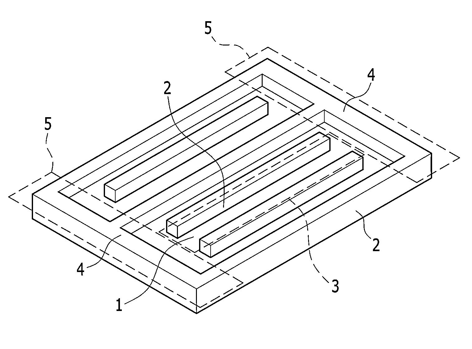
[0080](1) An 8-inch silicon wafer substrate is cleaned, and a positive photoresist is spin-coated at 2500 revolutions per minute (rpm) on the substrate and prebaked. The photoresist is exposed to light using a KrF scanner, and then baked and developed to prepare a photoresist pattern. By using the photoresist pattern as a mask, reactive ion etching is carried out to prepare a Si trench pattern having a trench and a latitudinal wall (trench width: 1000 nm, trench depth: 40 nm, trench length: 500 μm, and the height of the latitudinal wall: 40 nm) as shown in FIG. 2, and then the photoresist pattern is removed from therefrom.

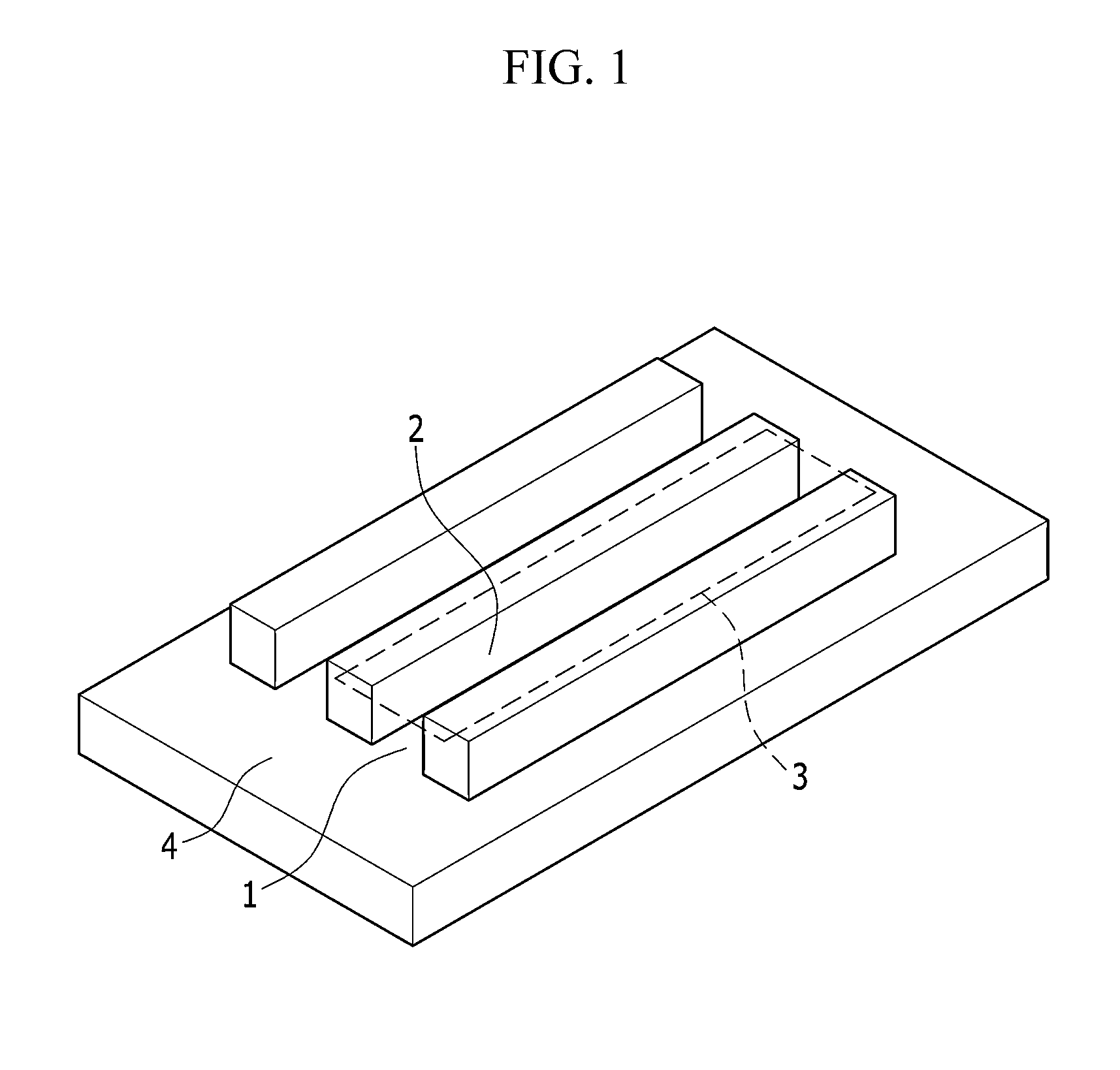
[0081](2) The Si trench pattern is cleaned with ultrasonic waves in acetone and exposed to UV ozone for 20 minutes. A polystyrene-b-polymethylmethacrylate (number average molecular weight: PS-b-PMMA 67k-21k, pattern period λo: 38 nm) solution (concentration: 0.8 wt %, solvent: toluene) is spin-coated on the cleaned Si trench pattern at 3000-4000 rpm for 60 seconds,...

example 2

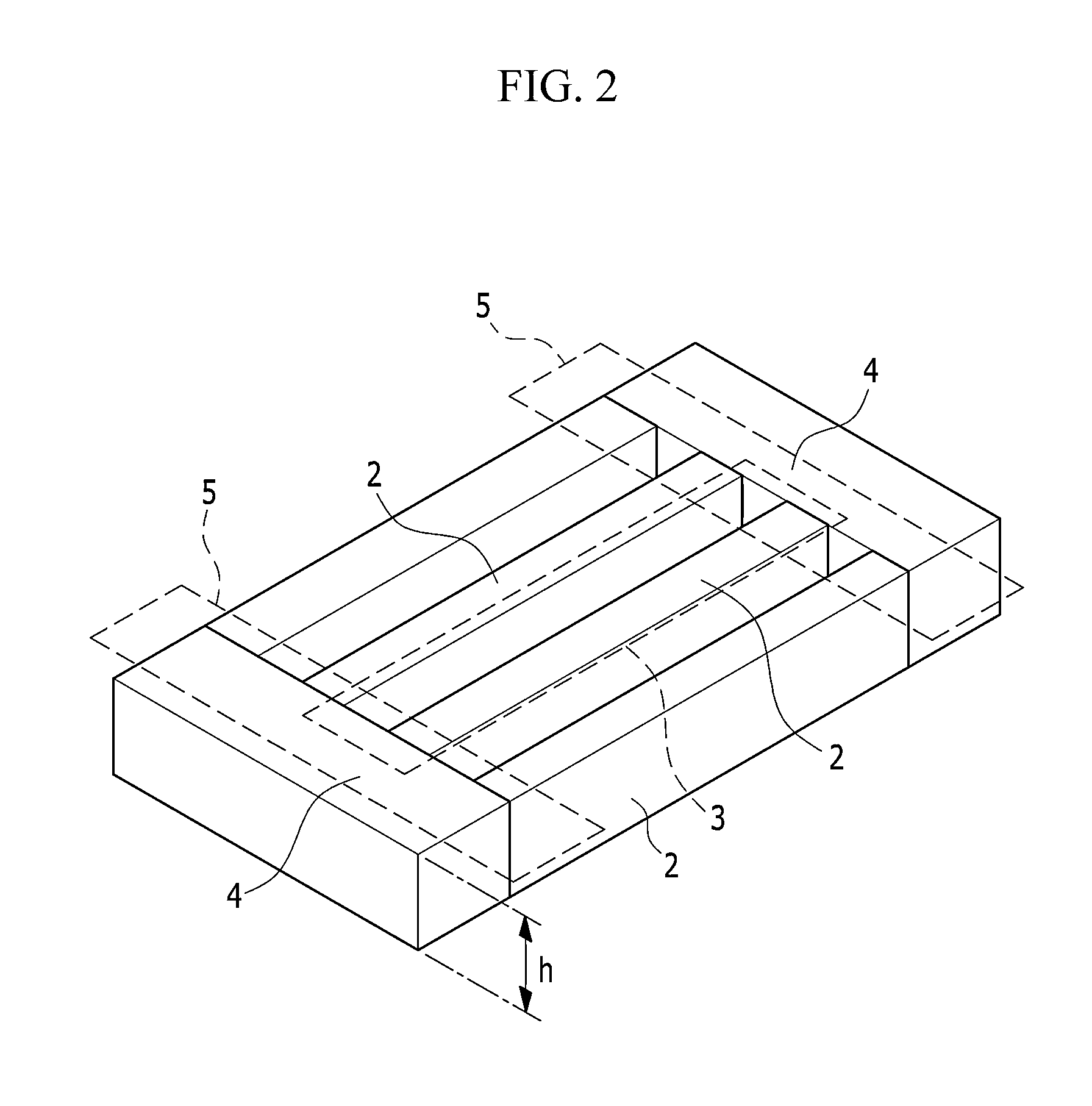
[0083]A cylinder pattern is formed in the same manner as set forth in Example 1, except for using the Si trench pattern including a trench and a latitudinal wall shown in FIG. 3 (trench width: 500 nm, trench depth: 40 nm, trench length: 1 cm, latitudinal wall height: 40 nm, and distance spaced apart from the trench end: 6 μm) and annealing it for 100 minutes. For each of the patterns, the dewetting area is calculated in a flat area 4 and in a trench 3. The results are provided in the following Table 1. FIG. 7 shows SEM images of the patterns thus obtained. The SEM images are obtained by using a SEM (model: S-4700, manufactured by Hitachi Co., Ltd.).


PUM

PropertyMeasurementUnit
distanceaaaaaaaaaa
thicknessaaaaaaaaaa
widthaaaaaaaaaa

Abstract

A method of patterning a block copolymer layer includes: providing a guide pattern on a surface of a substrate, the guide pattern including sidewalls each elongated in a longitudinal direction and spaced apart from each other, a trench defined by a bottom surface and facing surfaces of the sidewalls, and having a uniform width over an entire length thereof in the longitudinal direction, and a latitudinal wall perpendicular to the longitudinal direction of the trench; providing a block copolymer layer on the surface of the substrate; and annealing the block copolymer to cause self-assembly of the block copolymer and to direct the same in the trench. The block copolymer has a microphase-separation into anisotropic discrete domains aligned with a period λo in the trench by the annealing.

Description

CROSS-REFERENCE TO RELATED APPLICATIONS[0001]This application claims priority to Korean Patent Application No. 10-2012-0158701 filed on Dec. 31, 2012, and all the benefits accruing therefrom under 35 U.S.C. §119, the entire contents of which are incorporated herein by reference.BACKGROUND[0002]1. Field[0003]Provided is a method of patterning a block copolymer layer.[0004]2. Description of the Related Art[0005]Demands for lithography technology for forming a fine nano-sized pattern of a semiconductor memory or a logic circuit have increased in accordance with a decrease in a size of electronic devices including the semiconductor memory or the logic circuit, and an increase in a degree to which semiconductor devices have been integrated in electronic devices.[0006]Conventional photolithography technology has difficulties in realizing a fine nano-sized pattern. In particular, a nano-pattern of less than or equal to about 20 nanometers (nm) are difficult to manufacture, due to a wavelen...

Claims


Application Information

Patent Timeline
Patent Type & Authority Applications(United States)
IPC IPC(8): H01L21/02
CPCH01L21/02356H01L21/02118H01L21/0271H01L21/3081B81C1/00031B81C2201/0149B82Y10/00B82Y40/00H01L21/0273H01L21/0274H01L21/027
Inventor PARK, YOUN JUNGKOH, HAENG DEOGKIM, MI-JEONGJEONG, SEONG-JUN
Owner SAMSUNG ELECTRONICS CO LTD
Why Eureka
Try Eureka