Metal to metal bonding for stacked (3D) integrated circuits

a technology of integrated circuits and metals, applied in the direction of resistive material coating, superimposed coating process, liquid/solution decomposition chemical coating, etc., can solve the problems of over-interface thermal budget, increase in circuit resistance-capacitance (rc) delay and power consumption, and inability to continue scaling indefinitely, so as to achieve lower thermal budget and bond temperature

Active Publication Date: 2014-07-10
IBM CORP
View PDF1 Cites 19 Cited by
  • Summary
  • Abstract
  • Description
  • Claims
  • Application Information

AI Technical Summary

Benefits of technology

[0008]The present invention enables metal to metal bonding at lower bond temperature and time combination, enabling a lower thermal budget.

Problems solved by technology

But such scaling cannot continue indefinitely because devices are now approaching atomic dimensions.
Furthermore, as the density has increased, so has the complexity and length of the interconnect circuitry, causing increases in both circuit resistance-capacitance (RC) delay and power consumption.
Such stresses can cause distortions such as warpage of a silicon wafer.
Unfortunately, such conditions can exceed the thermal budget of delicate integrated circuitry which cannot be exposed, or at least not for extended time, to high temperature.
Bonding a 3D stack at lower temperatures would permit a wider selection of devices and materials, but has not been possible because, as noted above, conventional processing promotes grain growth such that a plated copper surface has a very low concentration of grain boundaries.
Even without a thermal anneal, thermodynamics drives grain growth and within a very short time converts the surface microstructure of plated copper such that metal to metal bonding at temperature below 350 C is impractical.

Method used


Image

  • Metal to metal bonding for stacked (3D) integrated circuits
  • Metal to metal bonding for stacked (3D) integrated circuits
  • Metal to metal bonding for stacked (3D) integrated circuits

Examples


Embodiment Construction

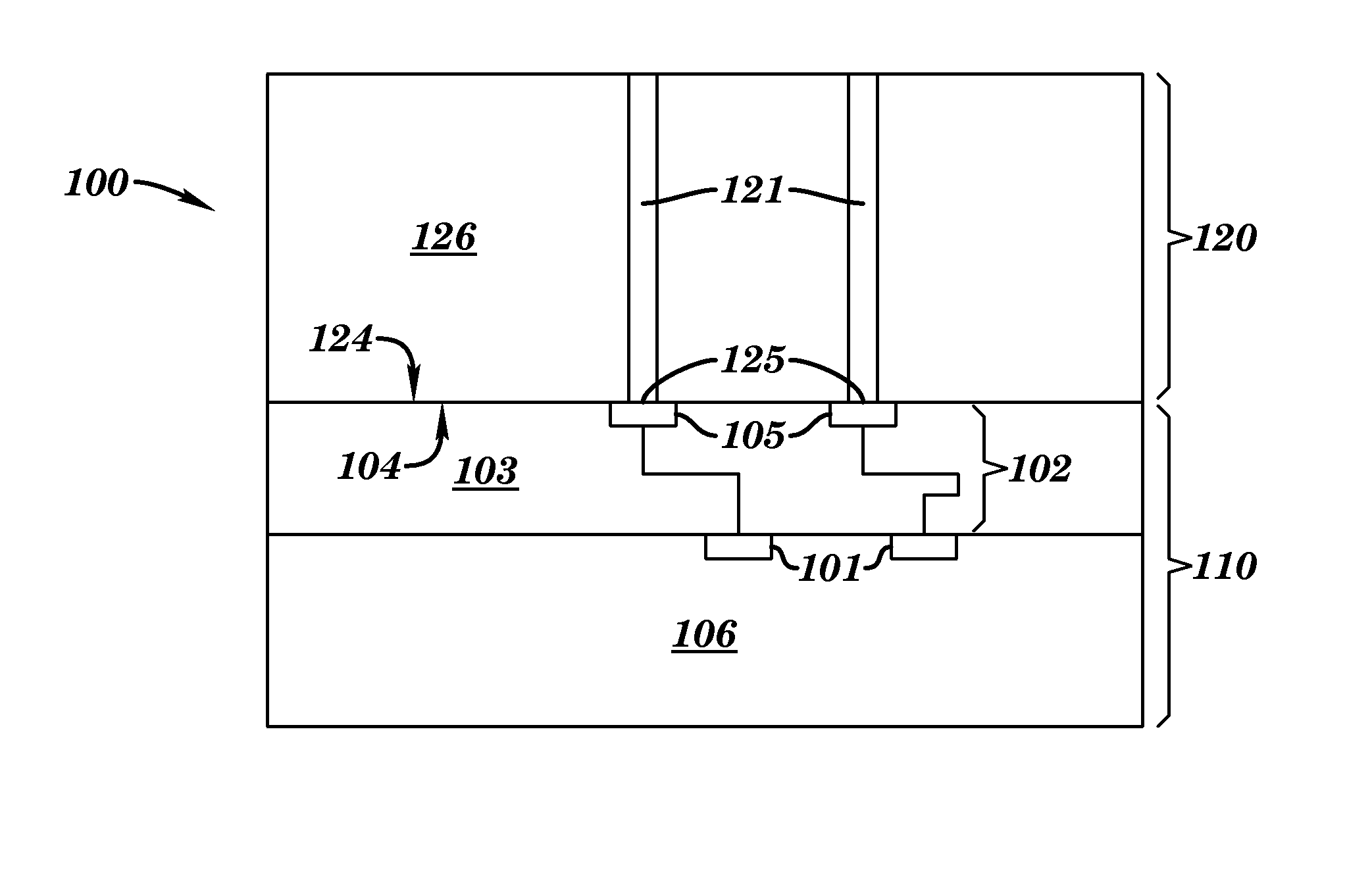
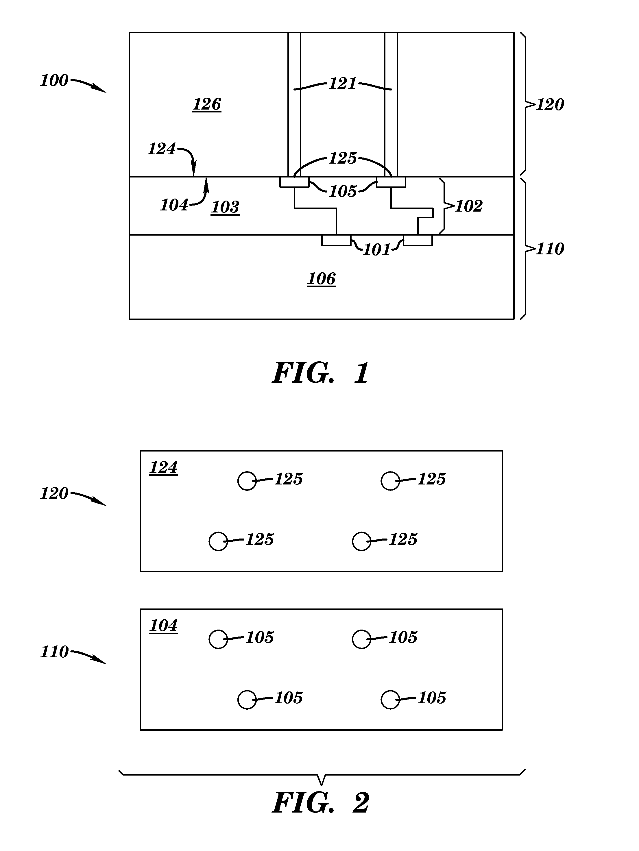
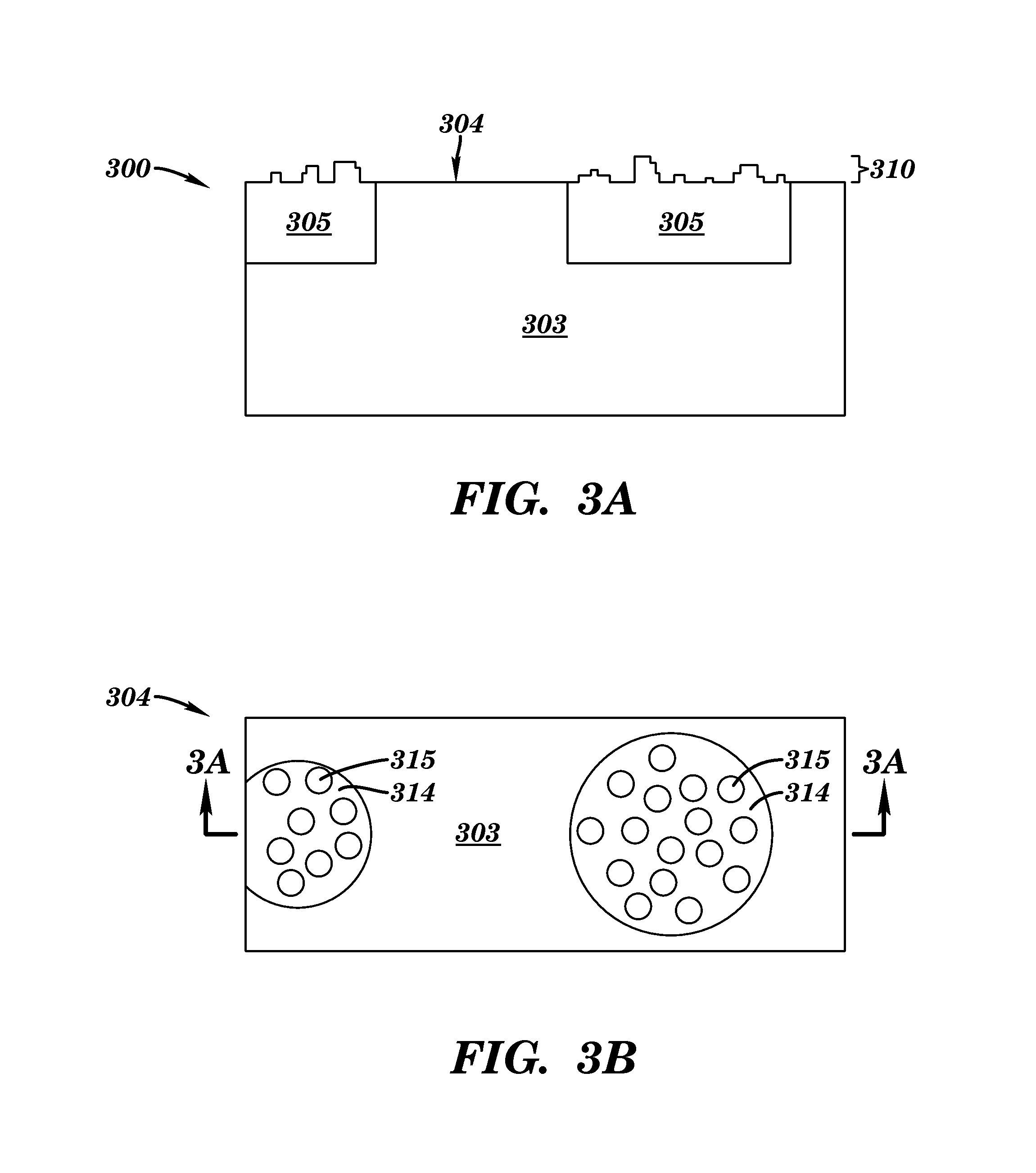
[0018]It will be understood that when an element as a layer, region or substrate is referred to as being “on” or “over” another element, it can be directly on the other element or intervening elements may also be present. In contrast, when an element is referred to as being “directly on” or “directly over” another element, there are no intervening elements present. Similarly, when an element is referred to as being “connected” or “coupled” to another element, it can be directly connected or coupled to the other element or intervening elements may be present. In contrast, when an element is referred to as being “directly connected” or “directly coupled” to another element, there are no intervening elements present. Additionally, to the extent a feature is described to be horizontal or vertical, that orientation is with respect to a generally planar major surface of the substrate which can be in the form of a wafer or disk.

[0019]The present invention promotes metal to metal bonding at...


PUM

PropertyMeasurementUnit
thicknessaaaaaaaaaa
grain sizeaaaaaaaaaa

Abstract

The present invention provides a stabilized fine textured metal microstructure that constitutes a durable activated surface usable for bonding a 3D stacked chip. A fine-grain layer that resists self anneal enables metal to metal bonding at moderate time and temperature and wider process flexibility.

Description

BACKGROUND[0001]The present invention relates generally to three dimensional (3D) integrated circuits, and more particularly to enabling the metal-to-metal bonding of integrated circuit substrates at low temperature and pressure.[0002]The semiconductor industry continues to drive toward greater functionality and speed of integrated circuits. For the most part, such improvements have been achieved by scaling the feature size such that more smaller devices can fit in a given area. But such scaling cannot continue indefinitely because devices are now approaching atomic dimensions. Furthermore, as the density has increased, so has the complexity and length of the interconnect circuitry, causing increases in both circuit resistance-capacitance (RC) delay and power consumption. Three-dimensional integrated circuits—that is, stacked chips bonded together—provides an opportunity to overcome these limitations.[0003]FIG. 1 illustrates a 3D stack 100 in which two semiconductor die are bonded t...

Claims


Application Information

Patent Timeline
Patent Type & Authority Applications(United States)
IPC IPC(8): H01L23/00H01L23/488
CPCH01L23/488H01L24/83H01L2224/03825H01L2224/80447H01L24/03H01L24/08H01L24/80H01L24/94H01L2224/0346H01L2224/03464H01L2224/038H01L2224/039H01L2224/05017H01L2224/05025H01L2224/05073H01L2224/05082H01L2224/05147H01L2224/05541H01L2224/05557H01L2224/0557H01L2224/05644H01L2224/05647H01L2224/05655H01L2224/08145H01L2224/80895H01L2224/94H01L2224/80203H01L2224/05005H01L2224/03829H01L2924/00014H01L25/50H01L2225/06513H01L25/0657H01L24/05H01L2924/3511H01L2224/80H01L2224/05155H01L2924/00012H01L2924/01046H01L2224/03616H01L2924/01047H01L2924/0105H01L2224/05552H01L23/5386H01L2224/05551H01L2224/05572H01L2924/1011H01L2224/83895H01L23/481H01L24/32H01L2224/27464H01L2224/27831H01L2224/32145H01L2224/32146H01L2225/06541
Inventor CHENG, TIEN-JENFAROOQ, MUKTA G.FITZSIMMONS, JOHN A.
Owner IBM CORP
Why Eureka
Try Eureka