Light-receiving device and method for producing the same

a light-receiving device and light-receiving technology, which is applied in the direction of semiconductor devices, photovoltaic energy generation, electrical apparatus, etc., can solve the problems of difficult to separate pixels, difficult to uniformly perform selective diffusion over large-diameter wafers, and difficult to planar-type photodiodes formed by selective diffusion, etc., to achieve satisfactory crystallinity, easy decomposition, and satisfactory crystallinity

Inactive Publication Date: 2014-07-17
SUMITOMO ELECTRIC IND LTD
View PDF4 Cites 14 Cited by
  • Summary
  • Abstract
  • Description
  • Claims
  • Application Information

AI Technical Summary

Benefits of technology

[0006]However, the planar-type photodiode formed by selective diffusion has problems described below.(1) When the light-receiving devices are formed on a large-diameter wafer, production efficiency can be enhanced. However, it is difficult to uniformly perform selective diffusion over the large-diameter wafer.(2) If a region in which impurity is not diffused is not sufficiently ensured, it is difficult to separate pixels. Therefore, the region in which impurity is not diffused is formed with a sufficient area between the pixels for reliably separating the pixels. As a result, the area fraction of an opening or selectively diffused region occupying an incident surface (that is, so-called “fill factor”) is reduced. Thus, sensitivity improvement is limited. In another respect, an increase in pixel pitch density is limited.
[0007]The mesa-type photodiodes have the advantage of having larger fill factors than the planar-type photodiodes. The mesa-type photodiodes have another advantage of having excellent controllability of positions of p-n junctions because p-n junctions are formed by epitaxial growth. The deviation of positions of p-n junctions changes the dependence of sensitivity and response speed on bias voltage, thus affecting the stability of properties of the photodiodes.
[0008]However, the mesa-type photodiode has a large leakage current that flows on a side surface of a mesa structure because of the exposure of a p-n junction at the side surface of the mesa structure. The leakage current causes the dark current of the photodiode. In particular, when the mesa structure is formed by dry etching, crystal damage occurs due to dry etching. The crystal damage due to dry etching tends to cause an increase in dark current. In general, dark current in the photodiode is required to be minimized. In order to reduce the dark current of a light-receiving device (photodiode), the light-receiving device may be cooled. Thus, a cooling mechanism, such as a Peltier element, may be provided to cool the light-receiving device. However, a light-receiving device having a cooling mechanism has demerits of increasing the device size and producing cost, for example. Therefore, a light-receiving element having a structure without a cooling mechanism, the structure by itself is a big feature of the light-receiving device. Even if a cooling mechanism is required, a low level of dark current makes it possible to reduce a cooling performance of the cooling mechanism, thereby reducing, for example, the size and cost of the cooling mechanism and the light-receiving device. It is thus important to form a mesa structure in which an edge of a p-n junction is not exposed to the atmosphere in order to reduce the dark current.

Problems solved by technology

However, the planar-type photodiode formed by selective diffusion has problems described below.
However, it is difficult to uniformly perform selective diffusion over the large-diameter wafer.
(2) If a region in which impurity is not diffused is not sufficiently ensured, it is difficult to separate pixels.
Thus, sensitivity improvement is limited.
In another respect, an increase in pixel pitch density is limited.
The deviation of positions of p-n junctions changes the dependence of sensitivity and response speed on bias voltage, thus affecting the stability of properties of the photodiodes.

Method used


Image

  • Light-receiving device and method for producing the same
  • Light-receiving device and method for producing the same
  • Light-receiving device and method for producing the same

Examples


first embodiment

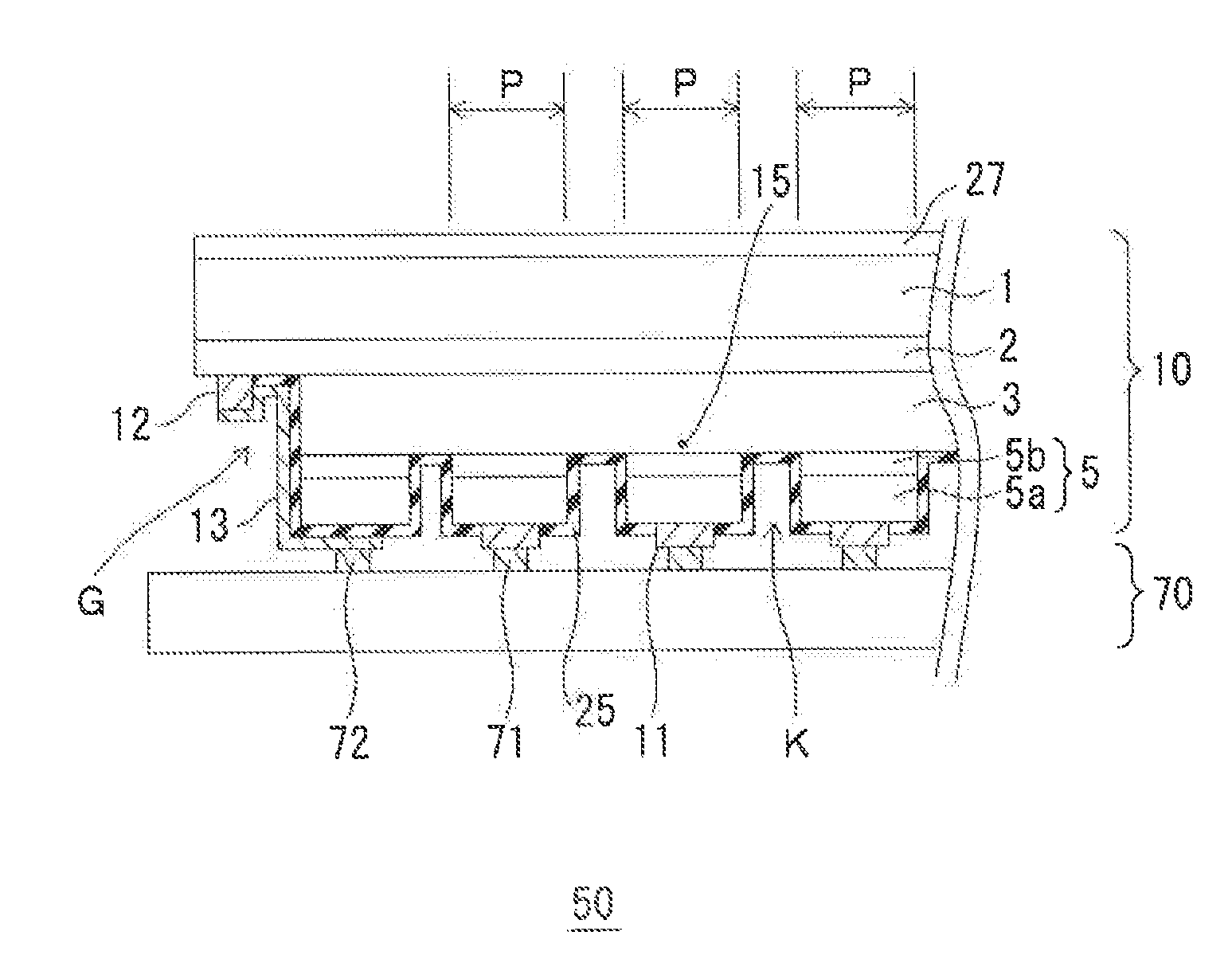
[0043]FIG. 1 illustrates a sensing apparatus 50 including a light-receiving device 10 and a read-out integrated circuit (ROIC) 70 connected to the light-receiving device 10. The light-receiving device 10 has a stacked semiconductor layer described below, (InP substrate 1 / n-type InP buffer layer 2 / light-receiving layer 3 / cap layer 5). The light-receiving layer 3 includes an undoped multi-quantum well (MQW) structure in which well layers and barrier layers are alternately stacked. Especially, the light-receiving layer 3 includes an undoped type-II multi-quantum well (MQW) structure. The light-receiving layer 3 including the type-II multi-quantum well (MQW) structure is explained hereinafter.

[0044]The cap layer 5 includes a p-type InGaAs contact layer 5a and an InGaAs concentration adjusting layer 5b adjacent to the p-type InGaAs contact layer 5a. A pixel electrode 11 is formed on the p-type InGaAs contact layer 5a and is in ohmic contact with the p-type InGaAs contact layer 5a. Zinc (...

modified embodiment

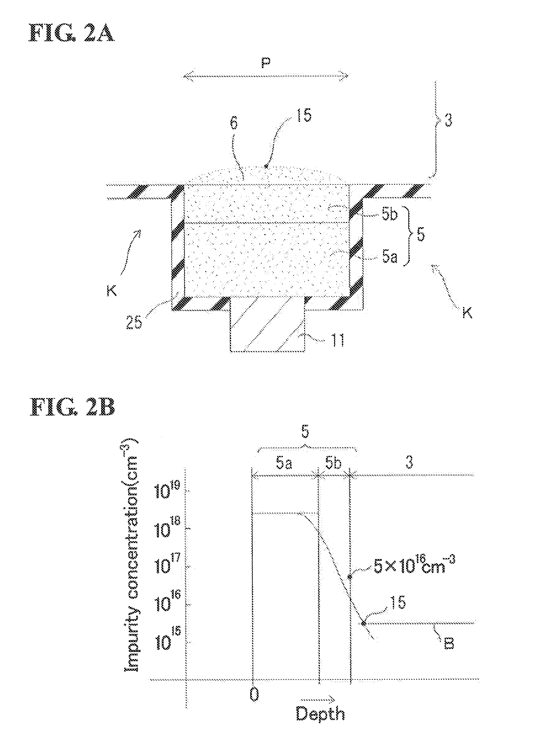
[0055]FIGS. 3A and 3B illustrate a modified embodiment of the light-receiving device 10 illustrated in FIG. 1. FIG. 3A is a partially enlarged cross-sectional view of the pixel P. FIG. 3B illustrates the in-depth distribution of the concentration of Zn serving as a p-type impurity. The difference between the modified embodiment and the light-receiving device 10 illustrated in FIGS. 1 and 2 is that a trench K is deepened in such a manner that the bottom of the trench K is located at a position 3b in the light-receiving layer 3. When the trench K is deepened to the light-receiving layer 3, the position of the bottom is located at a position in the light-receiving layer 3 away from the boundary between the concentration adjusting layer 5b and the light-receiving layer 3 by 2 / 10 or less of the thickness of the light-receiving layer. As illustrated in FIG. 3A, the deep mesa trench K increases a region where the depth position of the p-n junction 15 lies at a shallower depth than the dept...

second embodiment

[0065]FIG. 6 illustrates the sensing apparatus 50 in which the light-receiving device 10 according to a second embodiment is connected to the read-out integrated circuit (ROIC) 70. The difference from the light-receiving device 10 according to the first embodiment is that the cap layer 5 is formed of the p-type contact layer 5a alone without the concentration adjusting layer in this embodiment. The bottom of the trench K of the mesa structure is located at a position away from the upper surface of the light-receiving layer 3 by 20% or less of the thickness of the light-receiving layer 3.

[0066]FIG. 7A is a partially enlarged view of a pixel P illustrated in FIG. 6. FIG. 7A also illustrates a cross-sectional view of the distribution of Zn serving as a p-type impurity in the pixel P. In the embodiment, the pixels P are mechanically and structurally separated from each other by the trench K of the mesa structure. FIG. 7B illustrates the in-depth distribution of Zn concentration. In the ...


PUM


Abstract

A light-receiving device includes a light-receiving layer having an undoped multi-quantum well structure; a cap layer disposed on the light-receiving layer, the cap layer including a semiconductor layer doped with a p-type impurity; a mesa structure including the cap layer; a p-type region extending from the p-type semiconductor layer toward the light-receiving layer, the p-type region including the p-type impurity diffused from the semiconductor layer in the mesa structure; a p-n junction formed at an end of the p-type region; and an electrode disposed on the cap layer of the mesa structure. The mesa structure is defined by a trench surrounding the mesa. The trench has a bottom that reaches the vicinity of an upper surface of the light-receiving layer. The p-n junction is located in the light-receiving layer or at the boundary between the light-receiving layer and the cap layer disposed on the light-receiving layer.

Description

BACKGROUND OF THE INVENTION[0001]1. Field of the Invention[0002]The present invention relates to a light-receiving device and a method for producing the same.[0003]2. Description of the Related Art[0004]Living bodies, such as animals and plants, and substances, such as gases associated with the environment, have the characteristics of absorbing specific light in the infrared region including the near-infrared light with a wavelength of about 2 μm to 10 μm. In order to detect the absorption spectra of the substances such as gases associated with environments or organisms such as animals and plants, infrared light-receiving devices and infrared sensing devices including such infrared light-receiving devices are under development. In particular, in the near-infrared to infrared region, the photosensitivity to long-wavelength light is being improved. Here, the infrared light-receiving devices include a light-receiving layer composed of a III-V group compound semiconductor. In the light-...

Claims


Application Information

Patent Timeline
Patent Type & Authority Applications(United States)
IPC IPC(8): H01L33/06H01L33/30H01L33/20
CPCH01L33/06H01L33/30H01L33/20H01L27/1446H01L31/035236H01L31/1035H01L31/105H01L31/109H01L31/1844H01L31/00H01L31/03046H01L31/035263Y02E10/544
Inventor IGUCHI, YASUHIRONAGAI, YOUICHI
Owner SUMITOMO ELECTRIC IND LTD
Why Eureka
Try Eureka