Am-ewod device and method of driving with variable voltage ac driving

a technology of amewod and ac driving, which is applied in the field of active matrix electrowettingondielectric (amewod), can solve the problems of not disclosing circuit embodiments, and achieve the effects of reducing surface contamination, minimizing power consumption of the device, and improving device reliability

Active Publication Date: 2014-07-24
SHARP LIFE SCI EU LTD
View PDF2 Cites 28 Cited by
  • Summary
  • Abstract
  • Description
  • Claims
  • Application Information

AI Technical Summary

Benefits of technology

[0023]An advantage of the invention is that certain droplet operations (in particular move, merge and mix) can be undertaken with lower actuation voltages than are required for certain other droplet operations (mix, split). Performing droplet operations with a lower actuation voltage when possible helps to improve device reliability by preserving the oil layer, reducing surface contamination (bio-fouling) and minimizing power consumption by the device.
[0024]Accordingly, an aspect of the invention is an active matrix electrowetting on dielectric (AM-EWOD) device. Embodiments of the AM-EWOD device include a substrate electrode, and a plurality of array elements, each array element including an array element electrode. First circuitry is configured to supply a first time varying signal V1 to at least a portion of the array element electrodes, and second circuitry is configured to supply a second time varying signal V2 to the substrate electrode, wherein an actuation voltage is defined by a potential difference between V2 and V1. The first circuitry further is configured to adjust the amplitude of V1 to adjust the actuation voltage. The amplitude of V1 may be adjusted to adjust the actuation voltage while the amplitude of V2 remains unchanged.
[0025]Another aspect of the invention is a method of controlling an actuation voltage to be applied to a plurality of array elements of an active matrix electrowetting on dielectric (AM-EWOD) device, the AM-EWOD device having a substrate electrode and a plurality of array elements, each array element including an array element electrode, wherein the actuation voltage is defined by a potential difference between the substrate electrode and the array element electrodes. Embodiments of the method of controlling the actuation voltage include the steps of: supplying a first time varying signal V1 to at least a portion of the array element electrodes, supplying a second time varying signal V2 to the substrate electrode, and controlling the actuation voltage by adjusting the amplitude of V1 to adjust the actuation voltage. The amplitude of V1 may be adjusted to adjust the actuation voltage while the amplitude of V2 remains unchanged.

Problems solved by technology

A disadvantage of U.S. Pat. No. 7,163,612 is that it does not disclose any circuit embodiments for realizing the TFT backplane of the AM-EWOD.

Method used


Image

  • Am-ewod device and method of driving with variable voltage ac driving
  • Am-ewod device and method of driving with variable voltage ac driving
  • Am-ewod device and method of driving with variable voltage ac driving

Examples


first embodiment

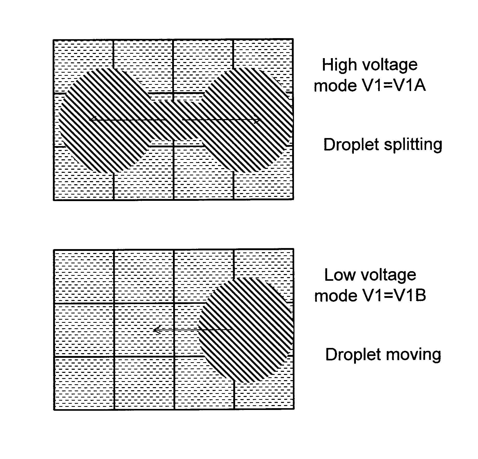
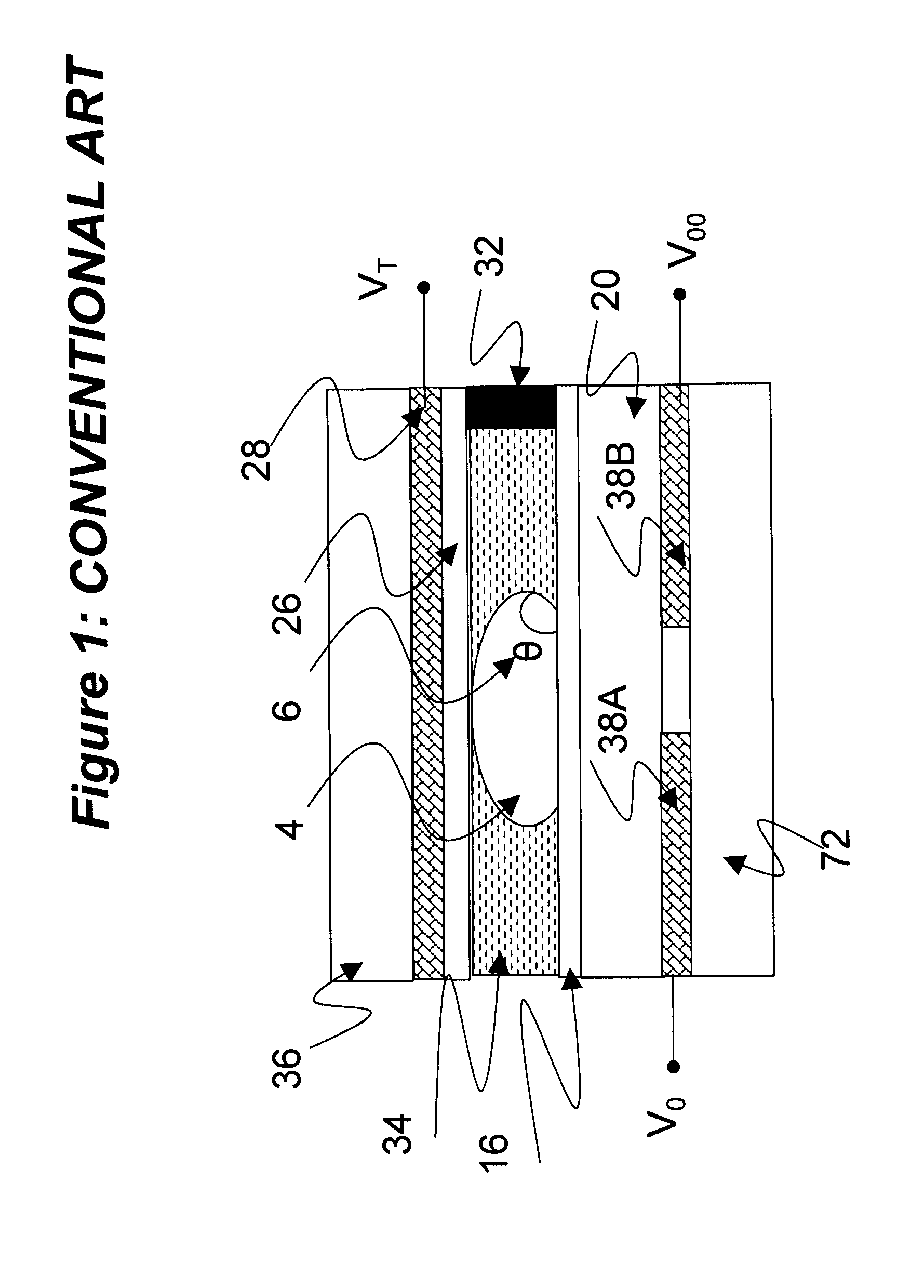
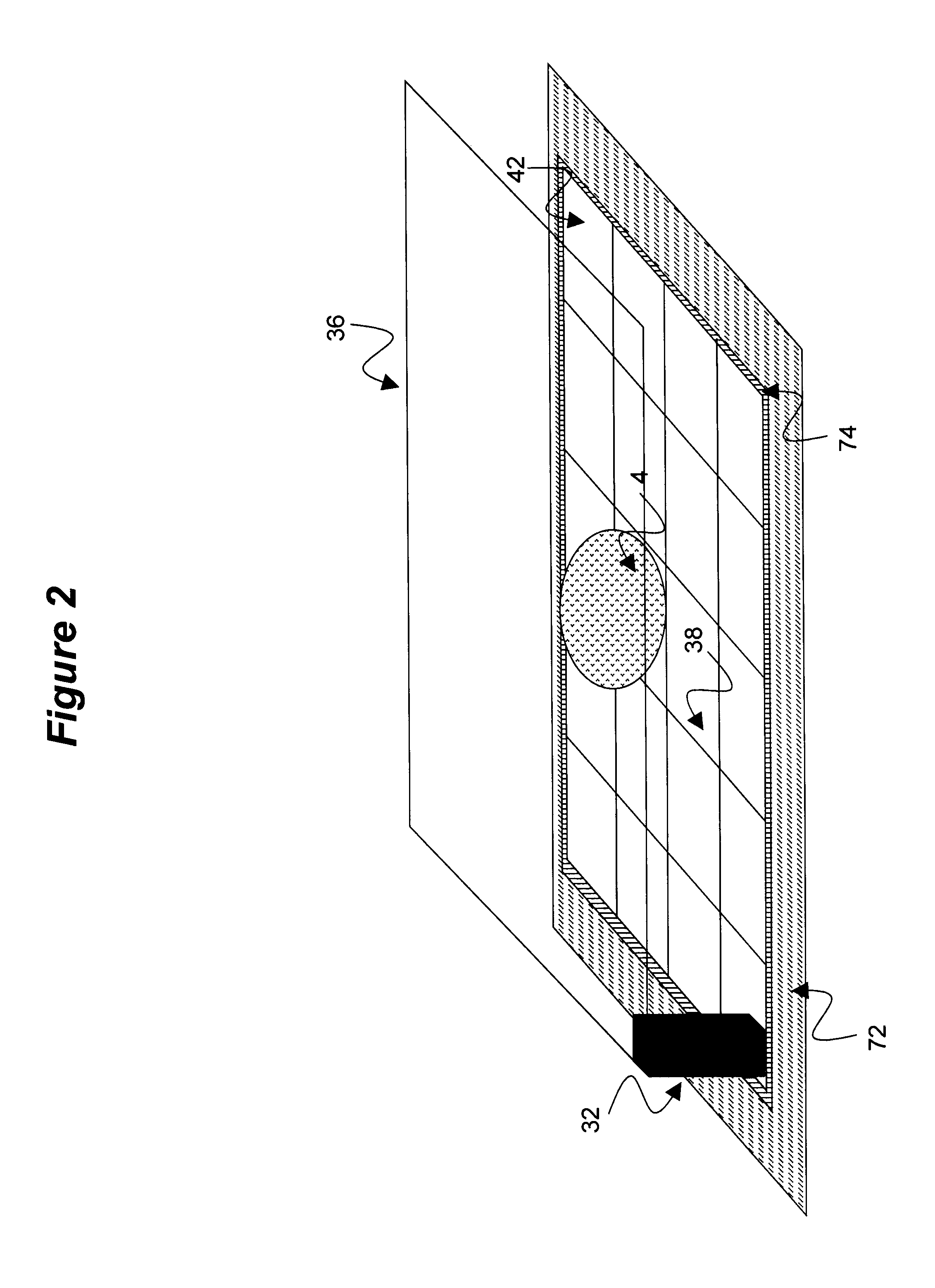
[0084]FIG. 5 is a schematic diagram depicting an exemplary configuration of the array element circuit 84 according to a The remainder of the AM-EWOD device is of the standard construction previously described with respect to FIGS. 2-4 and includes a top substrate 36 having a top substrate electrode 28.

[0085]In the exemplary configuration of FIG. 5, each array element circuit 84 contains:[0086]A memory element 100[0087]First circuitry including a first analogue switch 106[0088]Second circuitry including a second analogue switch 108[0089]A switch transistor 110.

[0090]The array element may also optionally contain[0091]A sensor circuit 116.

The array element circuit 84 is connected as follows:

[0092]The input DATA, which may be common to all elements in the same column of the array, is connected to the DATA input of the memory element 100. The input ENABLE, which may be common to all elements in the same row of the array, is connected to the input ENABLE of the memory element 100. The ou...

second embodiment

[0135]FIG. 10 is a schematic diagram depicting an example design of a suitable first signal generation circuit 88 in accordance with the The first signal generation circuit 88 includes the following components:[0136]A first level shifter circuit 90A of standard construction known to those of ordinary skill in the art; and[0137]A second level shifter circuit 90B of standard construction also known to those of ordinary skill in the art.

The signal generation 88 circuit has inputs S1, VBIAS1, VBIAS2, VBIAS3 and VBIAS4.

[0138]The first signal generation circuit 88 is connected as follows:

[0139]The input VBIAS1 is connected to the input VH of first level shifter circuit 90A. The input VBIAS2 is connected to the input VL of the first level shifter circuit 90A. The input VBIAS3 is connected to the input VH of the second level shifter circuit 90B. The input VBIAS4 is connected to the input VL of the second level shifter circuit 90B. The input S1 is connected to the inputs VIN of first level ...


PUM

PropertyMeasurementUnit
actuation voltagesaaaaaaaaaa
voltageaaaaaaaaaa
time varyingaaaaaaaaaa

Abstract

An active matrix electrowetting on dielectric (AM-EWOD) device includes a substrate electrode and a plurality of array elements, each array element including an array element electrode. The AM-EWOD device further includes thin film electronics disposed on a substrate. The thin film electronics includes first circuitry configured to supply a first time varying signal V1 to the array element electrodes, and second circuitry configured to supply a second time varying signal V2 to the substrate electrode. An actuation voltage is defined by a potential difference between V2 and V1, and the first circuitry further is configured to adjust the amplitude of V1 to adjust the actuation voltage. V1 may be adjusted to adjust the actuation voltage while V2 remains unchanged. The actuation voltage may be controlled to operate the AM-EWOD device between high and low voltage modes of operation in accordance with different droplet manipulation operations to be performed.

Description

TECHNICAL FIELD[0001]The present invention relates to active matrix arrays and elements thereof. In a particular aspect, the present invention relates to digital microfluidics, and more specifically to Active Matrix Electrowetting-On-Dielectric (AM-EWOD). Electrowetting-On-Dielectric (EWOD) is a known technique for manipulating droplets of fluid on an array. Active Matrix EWOD (AM-EWOD) refers to implementation of EWOD in an active matrix array, for example by using thin film transistors (TFTs). The invention further relates to methods of driving such a device.BACKGROUND ART[0002]Electrowetting on dielectric (EWOD) is a well known technique for manipulating droplets of fluid by application of an electric field. It is thus a candidate technology for digital microfluidics for lab-on-a-chip technology. An introduction to the basic principles of the technology can be found in “Digital microfluidics: is a true lab-on-a-chip possible?”, R. B. Fair, Microfluid Nanofluid (2007) 3:245-281).[...

Claims


Application Information

Patent Timeline
Patent Type & Authority Applications(United States)
IPC IPC(8): C25B15/00
CPCC25B15/00B01L3/502792G09G3/348B01L2200/0673B01L2300/0645B01L2300/0816B01L2300/089B01L2300/161B01L2400/0427G09G2230/00G09G2300/0819G09G2300/0857G09G2320/0693
Inventor HADWEN, BENJAMIN JAMES
Owner SHARP LIFE SCI EU LTD
Why Eureka
Try Eureka