Drive circuit and method for a gated semiconductor switching device

a gated semiconductor and driving circuit technology, applied in electronic switching, oscillator generators, pulse techniques, etc., can solve problems affecting device life, and achieve the effect of reducing increasing the switching speed of the gated semiconductor switching devi

Active Publication Date: 2014-07-24
E2V TECH (UK) LTD
View PDF10 Cites 9 Cited by
  • Summary
  • Abstract
  • Description
  • Claims
  • Application Information

AI Technical Summary

Benefits of technology

[0020]Conveniently, the phase of the mutual inductance increases a switching speed of the gated semiconductor switching device.
[0021]Alternatively, the phase of the mutual inductance decreases a switching speed of the gated semiconductor switching device.
[0029]Conveniently the method comprises providing a phase connection of the mutual inductance which increases a switching speed of the gated semiconductor switching device.
[0030]Alternatively, the method comprises providing a phase connection of the mutual inductance which decreases a switching speed of the gated semiconductor switching device.

Problems solved by technology

This is effective in increasing switching speed but is very stressful on the MOSFETs since it pushes the gate-source voltage to its very limit, usually only ±20V, and this can affect device life.
However, this solution requires a gate drive current source and the insertion of a source resistance.

Method used


Image

  • Drive circuit and method for a gated semiconductor switching device
  • Drive circuit and method for a gated semiconductor switching device
  • Drive circuit and method for a gated semiconductor switching device

Examples


Embodiment Construction

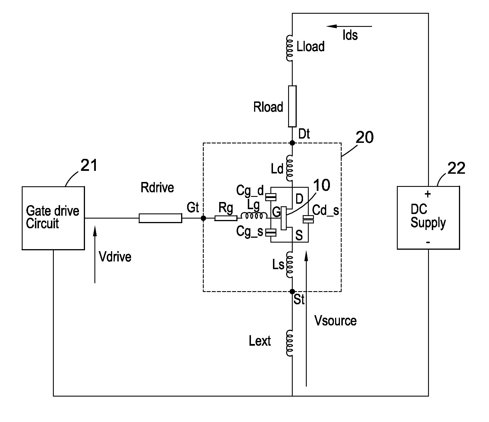
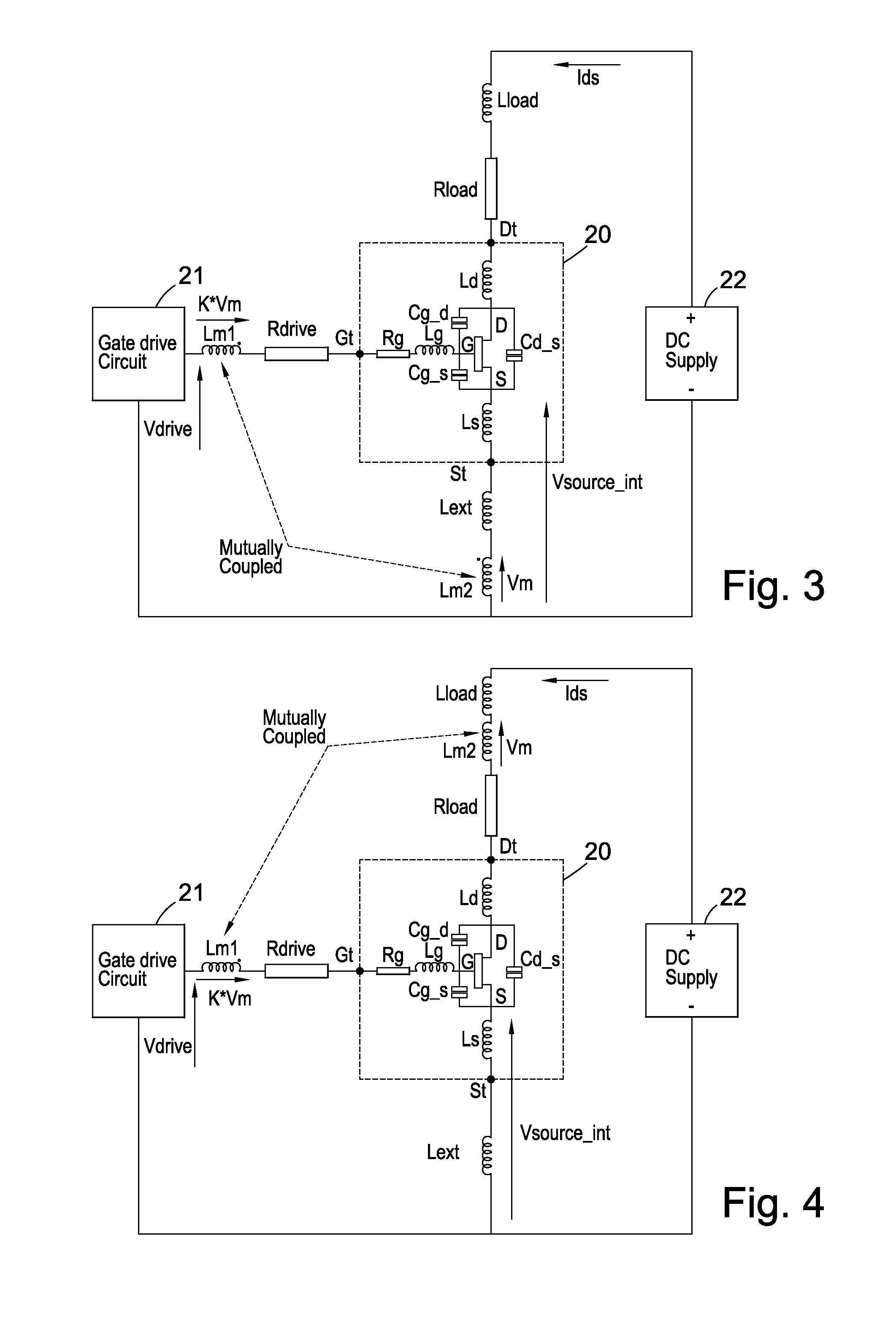
[0039]Referring to FIG. 3, a first embodiment of a drive circuit according to the invention includes, in addition to the components in the prior art circuit of FIG. 2, a small inductance Lm2 relative to the source inductance Ls, typically within a range of 0.5 nH to 2 nH, in series with the external inductance Lext between the DC supply 22 and the external source package terminal St. The inductance Lm2 is mutually coupled to another inductance Lm1 connected in series with the drive resistance Rdrive between the external gate terminal Gt and the gate drive circuit 21. A voltage Vm across inductance Lm2 induces a voltage K*Vm across the inductance Lm1 suitably phased to add in series with the drive voltage Vdrive applied to the external gate package terminal. A value of K can be selected so that a suitably large voltage is added to the drive voltage Vdrive to compensate for the effect of a voltage Vsource_int across the source inductance Ls, the external inductance Lext and the mutual...


PUM


Abstract

Drive circuit and method for a gated semiconductor switching device A drive circuit and method for a gated semiconductor switching device (10) comprising providing coupling such as a mutual inductance between a gate drive circuit (21) for the device and a drain to source current supply circuit (22) for the device in order to change a gate voltage provided by the gate drive circuit dependent on a rate of change of a current in the drain to source current supply circuit. The change in gate voltage has a magnitude and phase arranged to increase or decrease a switching speed of the gated semiconductor switching device.

Description

[0001]This invention relates to a drive circuit and method for a gated semiconductor switching device and in particular for a MOSFET.BACKGROUND[0002]Problems which have to be overcome in fast MOSFET switching are discussed in “Gate Drive Characteristics and Requirements for HEXFET™ Power MOSFETs ” International Rectifier Application Note AN-937, available from International Rectifier, 101 N Sepulveda Blvd., El Segundo, Calif. 90245, USA, which covers key requirements for driving MOSFETs.[0003]An equivalent circuit of a practical MOSFET 10 is shown in FIG. 1. A package 20 for the MOSFET comprises a source with an internal source connection S, a drain with an internal drain connection D and a gate with an internal gate connection G and with a corresponding respective external source package terminal St, external drain package terminal Dt and external gate package terminal Gt. Under most conditions when driving MOSFETs three stray capacitances between the internal connections, a gate-s...

Claims


Application Information

Patent Timeline
Patent Type & Authority Applications(United States)
IPC IPC(8): H03K3/012
CPCH03K3/012H03K17/0424H03K17/166H03K17/04206H03K17/0822
Inventor RICHARDSON, ROBERT
Owner E2V TECH (UK) LTD
Why Eureka
Try Eureka