Advanced Techniques for Improving High-Efficiency Optical Modulators

Active Publication Date: 2014-07-24
EOSPACE
View PDF11 Cites 11 Cited by
  • Summary
  • Abstract
  • Description
  • Claims
  • Application Information

AI Technical Summary

Benefits of technology

[0007]The invention describes advanced techniques to improve efficiency of an electro-optical modulator. The invention provides techniques to achieve a higher modulator efficiency by enhancing the elec

Problems solved by technology

However, the modulator efficiency is not as high as it should be.
The result is that the waveguides are relatively far from the central electrode of a CPW (Coplanar-waveguide) transmission-line electrode structure, leading to a non-optimum electro-optic field interaction inside the waveguide pair, which limits the achievable efficiency.
A simple r

Method used


Image

  • Advanced Techniques for Improving High-Efficiency Optical Modulators
  • Advanced Techniques for Improving High-Efficiency Optical Modulators
  • Advanced Techniques for Improving High-Efficiency Optical Modulators

Examples


Embodiment Construction

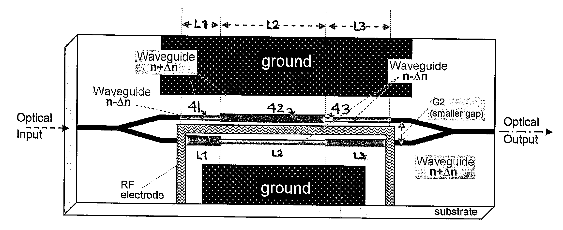
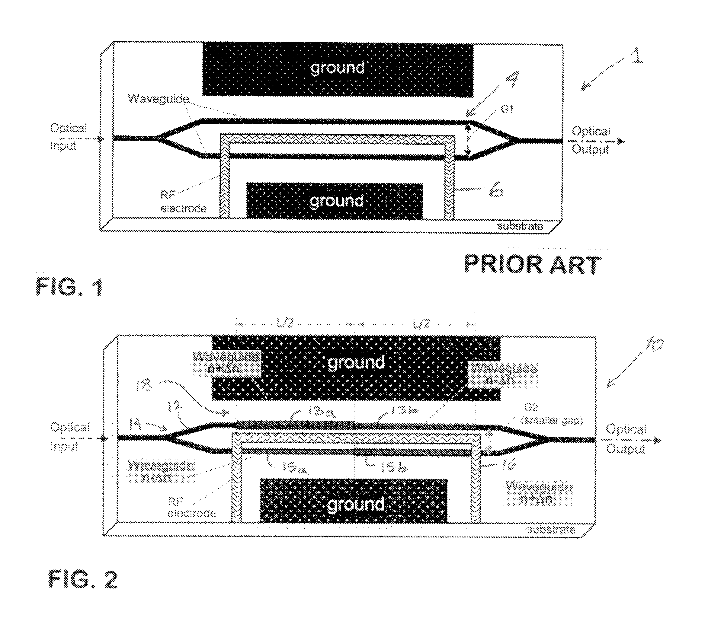
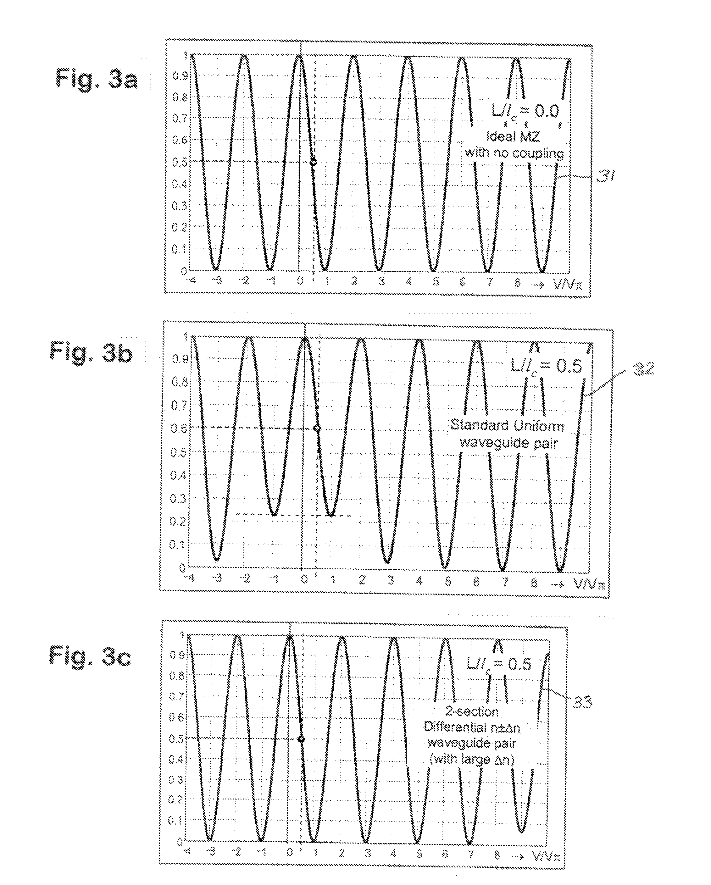
[0054]This invention describes advanced techniques to improve the efficiency of electro-optical waveguide modulators such as those fabricated on electro-optic material such as LiNbO3 substrate. These invention concepts can be applied to other types of modulators such as those fabricated on polymer, semiconductor, etc. These individual techniques can be applied separately or combined to realize higher efficiency modulators.

[0055]For clarity, these advanced techniques are described as applied to one of the most common and widely used optical modulators, namely wideband traveling-wave X-cut Y-propagation LiNbO3 Mach-Zehnder (MZ) electro-optic waveguide modulators, as prime examples.

[0056]First described is the creation and operation of this LiNbO3 MZ waveguide modulator followed by the inventions to improve this conventional device design.

[0057]Currently, one of the most widely-used optical modulators is a Mach-Zehnder (MZ) interferometer waveguide intensity modulator based on X-cut Y-...


PUM


Abstract

Improved optical interferometric modulators have a small waveguide spacing so that the waveguide pair are close to the central electrode, to enhance electro-optic interaction. Asymmetric waveguides with differential indices are used to effectively de-couple the waveguide pair. Multiple sections of asymmetric waveguide pairs with alternating differential indices are used to achieve chirp-free operation. Another version of the device utilizes transmission-line electrode that weave closer to one of the waveguide pair alternately between sections. Another version of the device utilizes waveguide structure that one of the waveguide is closer to the central electrode in alternate section. To improve efficiency further, a DC bias is provided on the outer electrodes configured as an RF-ground but DC-float electrodes. Another improvement is to have a slot is cut underneath the waveguide region to effectively reduce to thickness of the substrate. These improvements lead to higher modulator efficiency.

Description

[0001]This application claims the benefit of U.S. Provisional Application No. 61 / 656,341 filed Jun. 6, 2012, which is hereby incorporated by reference in its entirety as if fully set forth herein.BACKGROUND OF THE INVENTION[0002]A high-efficiency optical modulator is the key optical component used for converting an electrical signal to optical signal for fiber-optic or free-space transmissions. Such a device has a wide range of applications for broadband ‘digital’ fiber-optic telecommunication systems, and ‘analog’ signal transmissions such as fiber-optic antenna remoting, sensing, surveillance systems, and etc.[0003]The most common optical modulator product is the wideband electro-optic LiNbO3 device based on a Mach-Zehnder (MZ) interferometer singlemode waveguide structure with a traveling-wave transmission line electrode. These inventions are aimed at improving the design of these conventional MZ modulators.[0004]Optical waveguide modulators have been around for the last 40 years...

Claims


Application Information

Patent Timeline
IPC IPC(8): G02F1/225
CPCG02F1/225G02F1/0316G02F1/0356G02F1/2255G02F2201/127G02F1/212
Inventor THANIYAVARN, SUWAT
Owner EOSPACE
Why Eureka
Try Eureka