Methods of making patterned structures of materials, patterned structures of materials, and methods of using same

a technology of patterned structures and materials, applied in the field of patterning materials, can solve the problems of unattractive lithography community, significant swelling, intermixing or damage to the film of polymer a, and the limitation of only one self-assembled block copolymer domain size and pitch

Active Publication Date: 2014-07-24
CORNELL UNIVERSITY
View PDF2 Cites 30 Cited by
  • Summary
  • Abstract
  • Description
  • Claims
  • Application Information

AI Technical Summary

Benefits of technology

[0063]An advantage of the present invention is that the methods do not require use of a protective layer of material (e.g., perfluoroeicosane) that protects the layer(s) of organic polymer materials from solvents used during the process (e.g., solvents used in photoresist deposition, development, or removal (i.e., stripping)). Accordingly, in an embodiment the method does not require deposition of a protective layer of material on a layer of organic polymer material (e.g., a first or second layer of organic polymer material) prior to deposition of a layer of photoresist material.
[0064]Another advantage of the present invention is that methods provide a patterned layer or layers of organic polymer material such that the organic polymer materials are substantially unaffected by the process steps (e.g., process steps where the organic polymer materials are contacted by a solvent). By substantially unaffected it is meant that the physical properties (e.g., mechanical properties such as Young's modulus, hardness, toughness, film integrity (e.g., delamination, integrity, and pin hole density) and / or chemical properties (e.g., film composition) and / or electrical properties (e.g., conductivity, capacitance, and dielectric constant) and / or optical properties (e.g., refractive index, transparency, and haze), where the as deposited film exhibit such properties, are degraded by 10% or less. In various embodiments, the properties are degraded by 5% or less, 4% or less, 3% or less, 2% or less, and 1% or less. For example, if the film of organic polymer material is free of pin holes (as detectible by conventional analytical techniques) after deposition, it is free of detectible pin holes after the subsequent process steps (as detectible by conventional analytical techniques).
[0065]In an aspect, the present invention provides a layer or layers of patterned structures of two or more organic polymer materials on substrate. The patterned structures form a continuous layer or layers. For example, the layer or layers have a pattern of structures of a first organic polymer material and a pattern of structures of a second organic polymer material in the same layer.
[0066]In an aspect, the present invention provides uses of the layer or layers of polymer materials. For example, the layer or layers can be used in applications such as nanolithography or block copolymer lithography, organic electronic devices, semiconductors, bit patterned media, flash or other solid state memory, fuel cell membranes, light emitting diodes (LEDs) (e.g., organic light emitting diodes (OLEDs), thin film transistors (TFT), solar cells, sensors, microelectromechanical systems (MEMS), electrode patterning, nonvolatile memories, spin valves, and circuit elements (e.g., vias, resistors, capacitors, inductors, and the like). In an embodiment, a layer of polymer material(s) formed by the present invention is used as a hard-mask to transfer the pattern of the layer to another layer of material. In this embodiment, the organic polymer material.
[0067]The following examples are presented to illustrate the present invention. They are not intended to be limiting in any manner.

Problems solved by technology

If a particular application requires a stack of two different polymers, (e.g., Polymer B on top of Polymer A), attention must be paid to the interaction of Solvent B with the dry film of Polymer A. If Solvent B is miscible with Polymer A, the result is usually a significant amount of swelling, intermixing or damage to the film of Polymer A that may be undesirable for many applications.
The block copolymer community has been limited to the use of only one block copolymer per layer due to the damage and intermixing caused by the spin coating of another block copolymer solution on top of a previously deposited copolymer film.
The limitation of only one self-assembled block copolymer domain size and pitch is not attractive to the lithography community, which has grown used to the ability to print patterns of arbitrary shapes and sizes using photolithography.

Method used


Image

  • Methods of making patterned structures of materials, patterned structures of materials, and methods of using same
  • Methods of making patterned structures of materials, patterned structures of materials, and methods of using same
  • Methods of making patterned structures of materials, patterned structures of materials, and methods of using same

Examples


example 1

[0068]In the following example, two different block copolymers were spin-coated adjacent to each other in the same layer to demonstrate the CASP technique. Hydrofluoroether (HFE) (Novec™) solvents were obtained from 3M Co. and used as received. “OSCoR” photoresist was supplied by Orthogonal Inc. Triphenyl sulfonium triflate (TPST) photoacid generator was obtained from Aldrich and used as received. Tetramethoxymethylglycouril (TMMGU, “Powderlink 1174”) was donated by Cytec Industries. All other solvents were obtained from Aldrich and used as received. PαMS-b-PHOST block copolymers (Mn=53,000 g / mol, fPαMS˜34% (BCP1) and Mn=23,000 g / mol, fPαMS˜30% (BCP2) were synthesized as reported previously. Poly(styrene) with an —OH end group (PS—OH, Mn=10,000 g / mol, PDI=1.07) was obtained from Polymer Source (Dorval, Canada) and used as received. Single-polished Silicon wafers containing a ˜2 nm native oxide layer were obtained from WRS (Spring City, Pa.).

[0069]Silicon wafers cleaned with oxygen ...

example 2

[0078]In this example the non-interaction between the block copolymer film and hydrofluoroether (HFE) solvents was investigated for orthogonal processing

[0079]Materials. Hydrofluoroether solvents (HFEs, Novec™ Engineered Fluids) were obtained from 3M Corporation and used as received. Organic SemiConductor Resist (OSCoR) was supplied by Orthogonal Inc. Triphenyl sulfonium triflate (TPST, photoacid generator) was obtained from Sigma-Aldrich and used as received. Tetramethoxymethylglycouril (TMMGU, “Powderlink 1174”) was donated by Cytec Industries. All other solvents were obtained from Sigma-Aldrich and used as received. PαMS-b-PHOST block copolymers (Mn=53,000 g / mol, fPαMS˜34% (BCP1) and Mn=23,000 g / mol, fPαMS˜30% (BCP2) were synthesized according to known literature procedures. Hydroxyl-terminated polystyrene (PS—OH) was obtained from Polymer Source and used as received. Single-polished Silicon wafers with native oxide layer were obtained from WRS Materials.

[0080]Block Copolymer Fi...

example 3

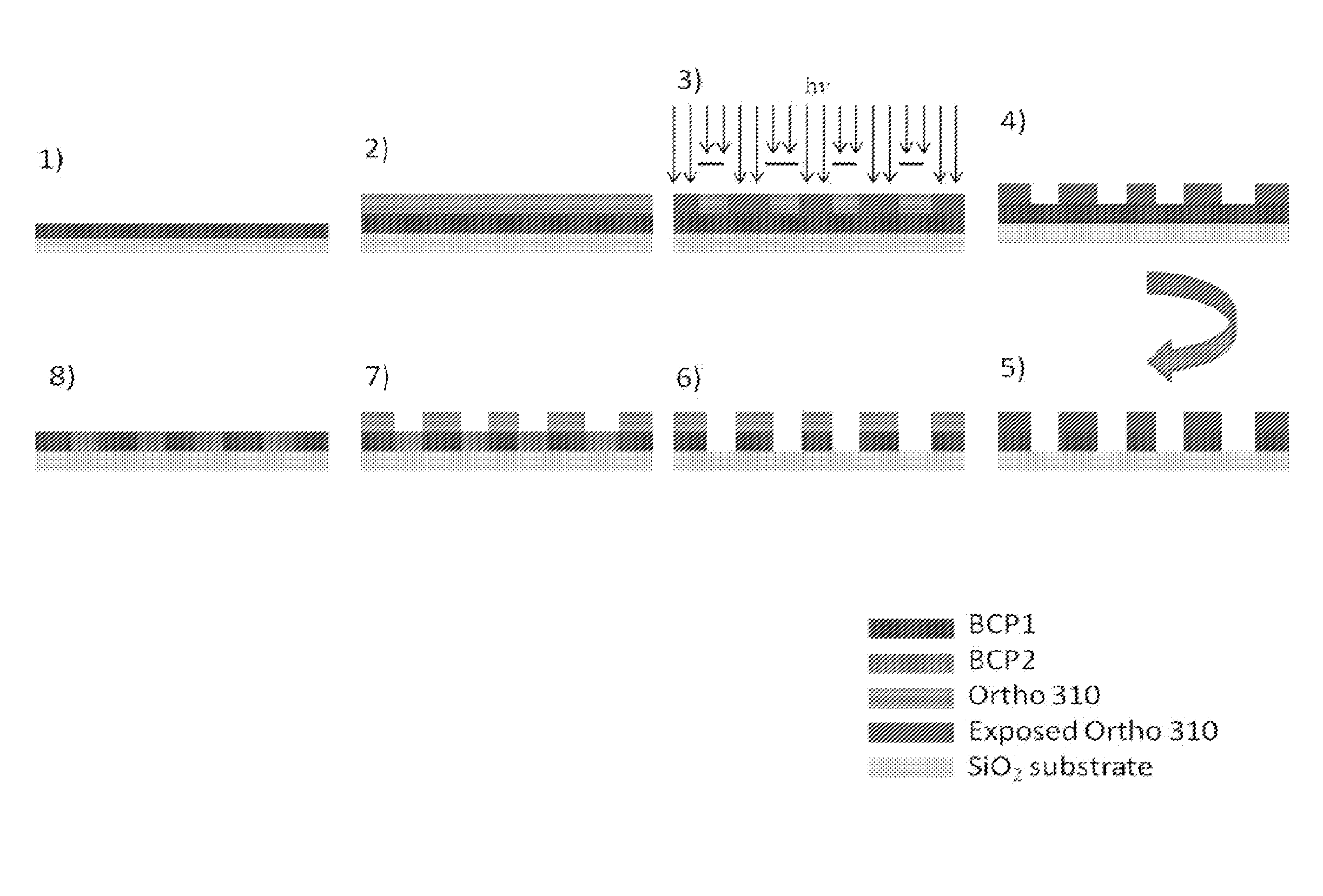
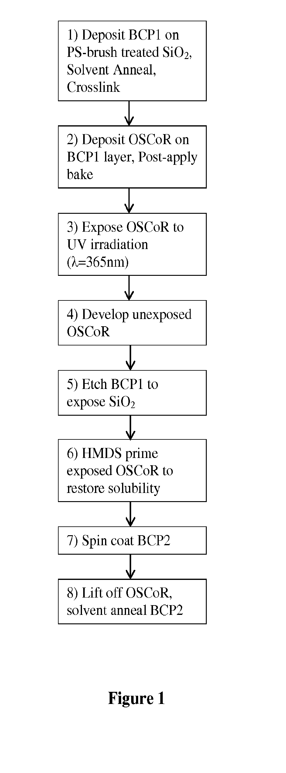
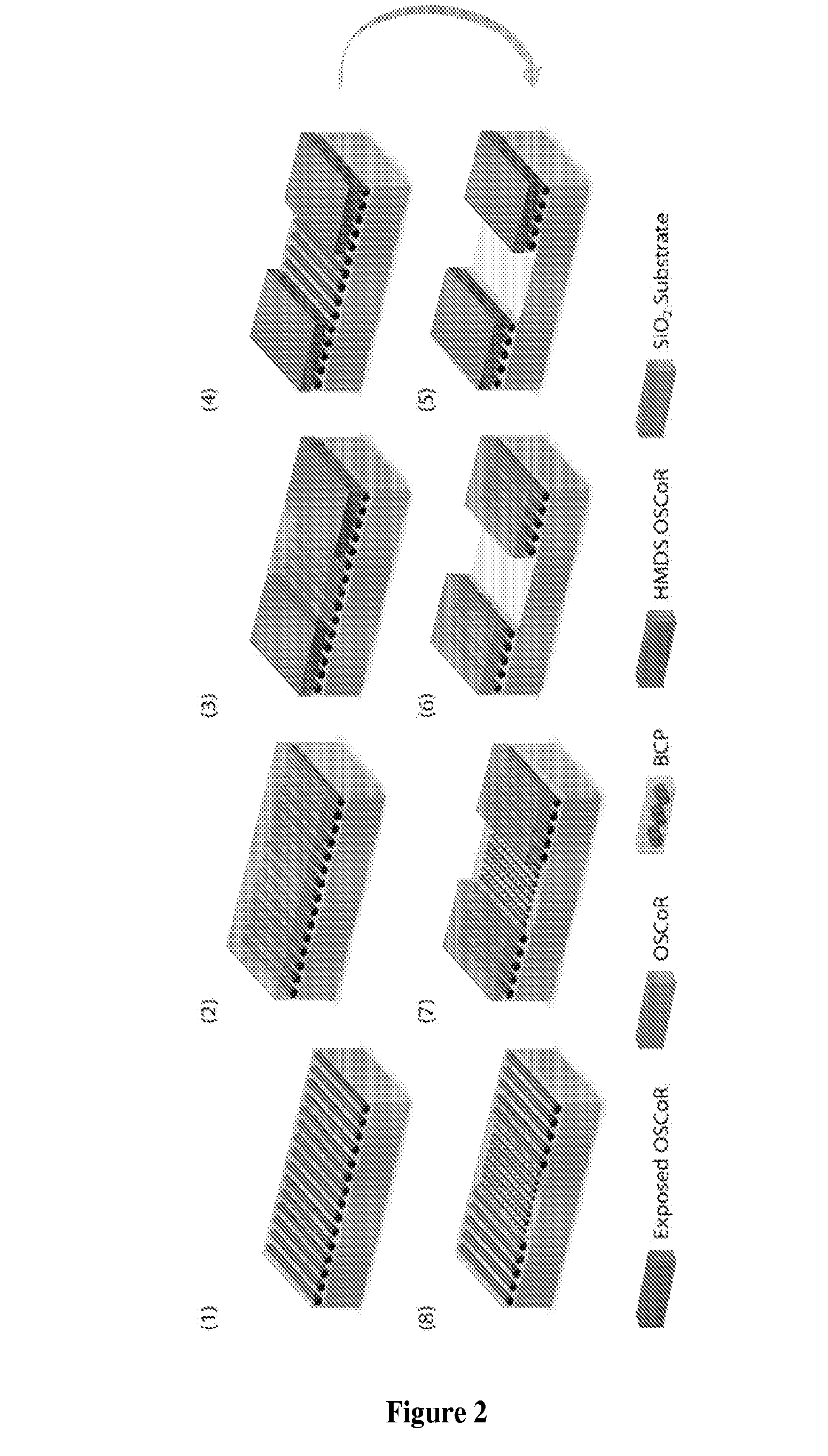
[0089]The following is an example of a method of the present invention.

Experimental Methods

[0090]Materials. Hydrofluoroether (HFE) (Novec™) solvents were obtained from 3M Corporation and used as received. Poly(1H,1H,2H,2H-perfluorodecyl methacrylate-ran-tert-butyl methacrylate) (P(FDMA-ran-TBMA), “Ortho 310”) photoresist was supplied by Orthogonal Inc. Triphenyl sulfonium triflate (TPST) photoacid generator was obtained from Aldrich and used as received. Tetramethoxymethylglycouril (TMMGU, “Powderlink 1174”) was donated by Cytec Industries. All other solvents were obtained from Aldrich and used as received. PαMS-b-PHOST block copolymers (Mn=53,000 g / mol, fαMS˜34% (BCP1) and Mn=23,000 g / mol, fPαMS˜30% (BCP2) were synthesized according to known literature procedures. Poly(styrene) with an ˜OH end group (PS—OH) was obtained from Polymer Source (Dorval, CA) and used as received. Single-polished Silicon wafers containing a ˜2 nm native oxide layer were obtained from WRS materials (Sprin...


PUM

PropertyMeasurementUnit
thickaaaaaaaaaa
thickaaaaaaaaaa
areaaaaaaaaaaa

Abstract

A method for forming patterns of organic polymer materials. The method can be used to form a layer with two patterned organic polymer materials. The photoresist and solvents used in the photoresist deposition and removal steps do not substantially affect the organic polymer materials.

Description

CROSS-REFERENCE TO RELATED APPLICATIONS[0001]This application claims priority to U.S. provisional patent application No. 61 / 454,015, filed Mar. 18, 2011, the disclosure of which is incorporated herein by reference.STATEMENT REGARDING FEDERALLY SPONSORED RESEARCH[0002]This invention was made with government support under grant number FA9550-09-1-0705 awarded by the Air Force Office of Scientific Research (AFOSR) MURI Program on new graphene materials technology. The United States Government has certain rights in the invention.FIELD OF THE INVENTION[0003]The present invention generally relates to methods of patterning materials. More particularly, the methods relate to patterning using a combination of additive and subtractive patterning steps (CASP).BACKGROUND OF THE INVENTION[0004]There are multiple ways to deposit functional polymer films. Spin coating has been used extensively in the field of electronics for its ability to spread solution-processable materials in smooth films over...

Claims


Application Information

Patent Timeline
Patent Type & Authority Applications(United States)
IPC IPC(8): G03F7/16H01L21/027
CPCH01L21/027G03F7/16B81C1/00031B81C2201/0149G03F7/0002G03F7/038Y10T428/24851
Inventor SCHWARTZ, EVAN L.CHAN, WEI MINLEE, JIN-KYUNTIWARI, SANDIPOBER, CHRISTOPHER K.
Owner CORNELL UNIVERSITY
Why Eureka
Try Eureka