Heat treatment apparatus and heat treatment method for heating substrate by irradiating substrate with flash of light

a heat treatment apparatus and heat treatment method technology, applied in lighting and heating apparatus, semiconductor/solid-state device testing/measurement, furnaces, etc., can solve problems such as uniform in-plane temperature distribution and much greater junction depth

Active Publication Date: 2014-07-24
DAINIPPON SCREEN MTG CO LTD
View PDF6 Cites 15 Cited by
  • Summary
  • Abstract
  • Description
  • Claims
  • Application Information

AI Technical Summary

Benefits of technology

[0023]The method causes the illuminance of a flash of light from a region of the arrangement where illuminance is low to become relatively high, thereby achieving the uniform in-plane temperature distribution of the substrate during flash irradiation.
[0024]It is therefore an object of the present invention to achieve a uniform in-plane temperature distribution of a substrate during flash irradiation.

Problems solved by technology

This results in a junction depth much greater than a required depth, which might constitute a hindrance to good device formation.
Even if a plurality of flash lamps emit light in a similar fashion, an actual flash lamp annealer has a problem such that nonuniformity in illuminance coming from an apparatus configuration problem results in the nonuniform in-plane temperature distribution of a semiconductor wafer during flash irradiation.

Method used


Image

  • Heat treatment apparatus and heat treatment method for heating substrate by irradiating substrate with flash of light
  • Heat treatment apparatus and heat treatment method for heating substrate by irradiating substrate with flash of light
  • Heat treatment apparatus and heat treatment method for heating substrate by irradiating substrate with flash of light

Examples


first preferred embodiment

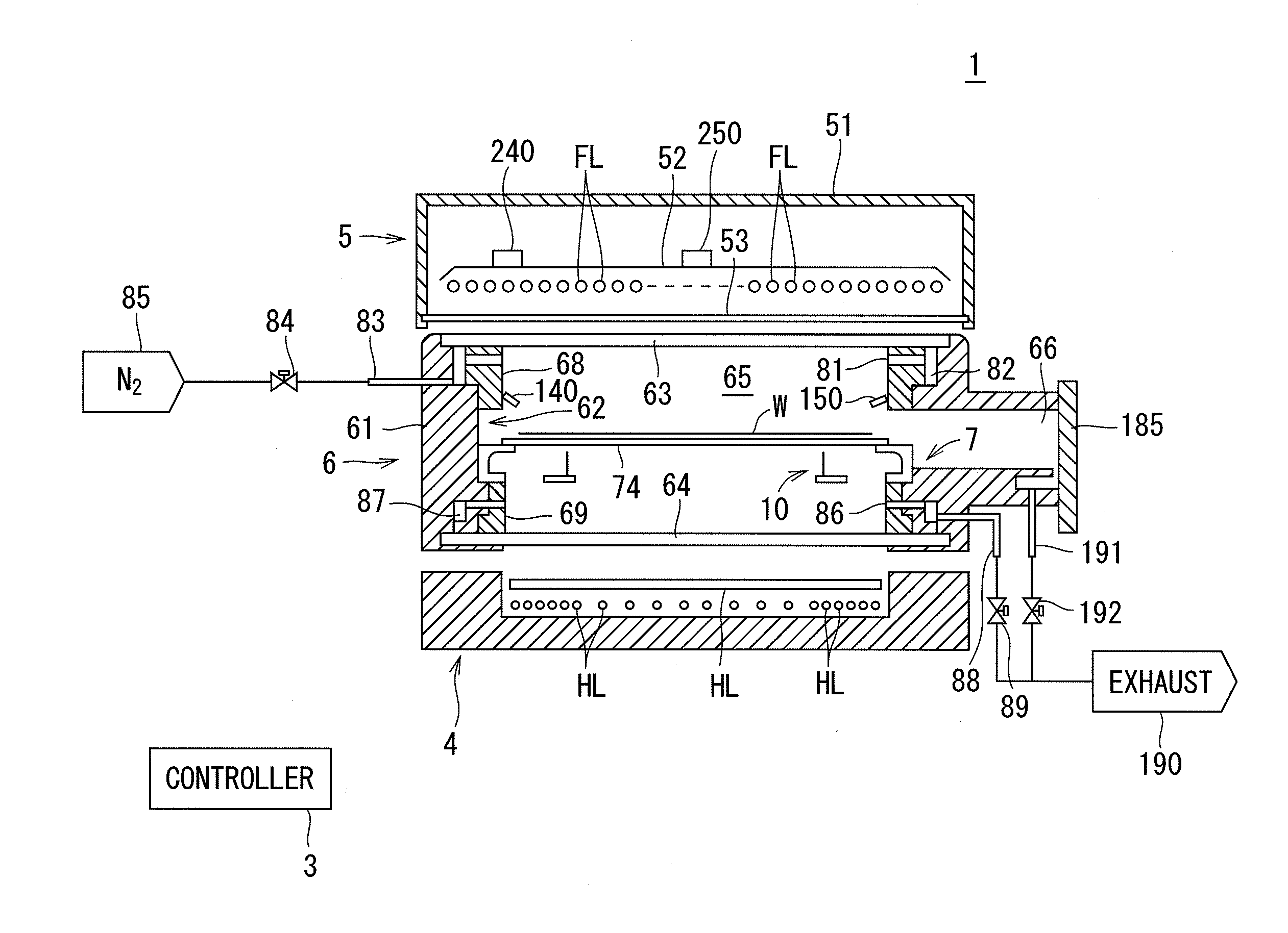
[0041]FIG. 1 is a longitudinal sectional view showing a configuration of a heat treatment apparatus 1 according to the present invention. The heat treatment apparatus 1 according to a first preferred embodiment of the present invention is a flash lamp annealer for irradiating a disk-shaped semiconductor wafer W serving as a substrate with a flash of light to heat the semiconductor wafer W. The size of the semiconductor wafer W to be treated is not particularly limited. For example, the semiconductor wafer W to be treated has a diameter of 300 mm and 450 mm. The semiconductor wafer W prior to the transport into the heat treatment apparatus 1 is implanted with impurities. The heat treatment apparatus 1 performs a heating treatment on the semiconductor wafer W to thereby activate the impurities implanted in the semiconductor wafer W.

[0042]The heat treatment apparatus 1 includes a chamber 6 for receiving a semiconductor wafer W therein, a flash heating part 5 including a plurality of bu...

second preferred embodiment

[0118]Next, a second preferred embodiment according to the present invention will be described. A heat treatment apparatus according to the second preferred embodiment is exactly identical in configuration with that according to the first preferred embodiment. A procedure for the treatment of a semiconductor wafer W according to the second preferred embodiment is generally similar to that according to the first preferred embodiment. The operations of the switching elements 96 and the charging voltages to the capacitors 93 are controlled in the first preferred embodiment, based on the result of measurement of the in-plane temperature distribution of the semiconductor wafer W. In the second preferred embodiment, similar control is exercised based on the result of measurement of an illuminance distribution of the arrangement of the 30 flash lamps FL. Specifically, the controller 3 controls the operations of the 30 switching elements 96 and the charging voltages applied from the chargin...


PUM


Abstract

A flash heating part in a heat treatment apparatus includes 30 built-in flash lamps, and irradiates a semiconductor wafer held by a holder in a chamber with a flash of light. Thirty switching elements are provided in a one-to-one correspondence with the 30 flash lamps. Each of the switching elements defines the waveform of current flowing through a corresponding one of the flash lamps by intermittently supplying electrical charge thereto. Radiation thermometers measure an in-plane temperature distribution of the semiconductor wafer during flash irradiation. Based on the results of measurement with the radiation thermometers, a controller individually controls the operations of the 30 switching elements to individually define the light emission patterns of the 30 flash lamps.

Description

BACKGROUND OF THE INVENTION[0001]1. Field of the Invention[0002]The present invention relates to a heat treatment apparatus and a heat treatment method for heating a thin plate-like precision electronic substrate such as a semiconductor wafer and a glass substrate for a liquid crystal display device (hereinafter referred to simply as a “substrate”) by irradiating the substrate with a flash of light.[0003]2. Description of the Background Art[0004]In the process of manufacturing a semiconductor device, impurity doping is an essential step for forming a pn junction in a semiconductor wafer. At present, it is common practice to perform impurity doping by an ion implantation process and a subsequent annealing process. The ion implantation process is a technique for causing ions of impurity elements such as boron (B), arsenic (As) and phosphorus (P) to collide against the semiconductor wafer of silicon with high acceleration voltage, thereby physically implanting the impurities into the s...

Claims


Application Information

Patent Timeline
Patent Type & Authority Applications(United States)
IPC IPC(8): H01L21/66H01L21/263H01L21/67
CPCH01L22/26H01L21/67248H01L21/67115H01L21/2636H01L21/324
Inventor KIYAMA, HIROKI
Owner DAINIPPON SCREEN MTG CO LTD
Why Eureka
Try Eureka