XRF measurement apparatus for detecting contaminations on the bevel of a wafer

a technology of x-ray fluorescence and measurement apparatus, which is applied in the direction of radiation measurement, instruments, material analysis, etc., can solve the problems of large signal level of contamination, and achieve the effect of quick and simple change of x-ray optics and simplified sample area chang

Active Publication Date: 2014-07-31
BRUKER AXS
View PDF25 Cites 0 Cited by
  • Summary
  • Abstract
  • Description
  • Claims
  • Application Information

AI Technical Summary

Benefits of technology

[0016]The invention proposes to use XRF on the bevel (edge) of a wafer, such as a silicon wafer, and to direct x-rays onto the bevel accordingly. Preferably, the (primary) x-ray hits only the bevel of the wafer, and not the flat side surface of the wafer when the bevel is analyzed. Further, the invention proposes to apply an x-ray source, in particular of micro-source type, with a high brilliance. This ensures that a sufficient signal level is achieved from possible contaminations, so contaminations can reliably be detected. The XRF measurement can be evaluated immediately, without delays for, for example, transporting a receptive carrier to a mass spectrometer. The inventive method is non-destructive and not likely to introduce new contaminations.
[0033]Also within the scope of the present invention is the use of an inventive apparatus as described above, for detecting contaminations on the bevel of a wafer, in particular a silicon wafer, by means of XRF. The XRF analysis is non-destructive and can give immediate results on the contamination level. Note that typical contaminations looked for by means of the invention include Al (from grippers) and Na (from salt contained in human sweat),In a preferred variant of the inventive use, a gallium L line is used for x-ray generation in the x-ray source. This has shown good results in practice; gallium can well be used in a metal jet, since gallium has a relatively low melting point of about 30° C. and therefore needs only a minimum of heating.

Problems solved by technology

This geometry results in larger signal levels from contaminations, as compared to incident primary beams closer to a perpendicular orientation.

Method used


Image

  • XRF measurement apparatus for detecting contaminations on the bevel of a wafer
  • XRF measurement apparatus for detecting contaminations on the bevel of a wafer
  • XRF measurement apparatus for detecting contaminations on the bevel of a wafer

Examples


Embodiment Construction

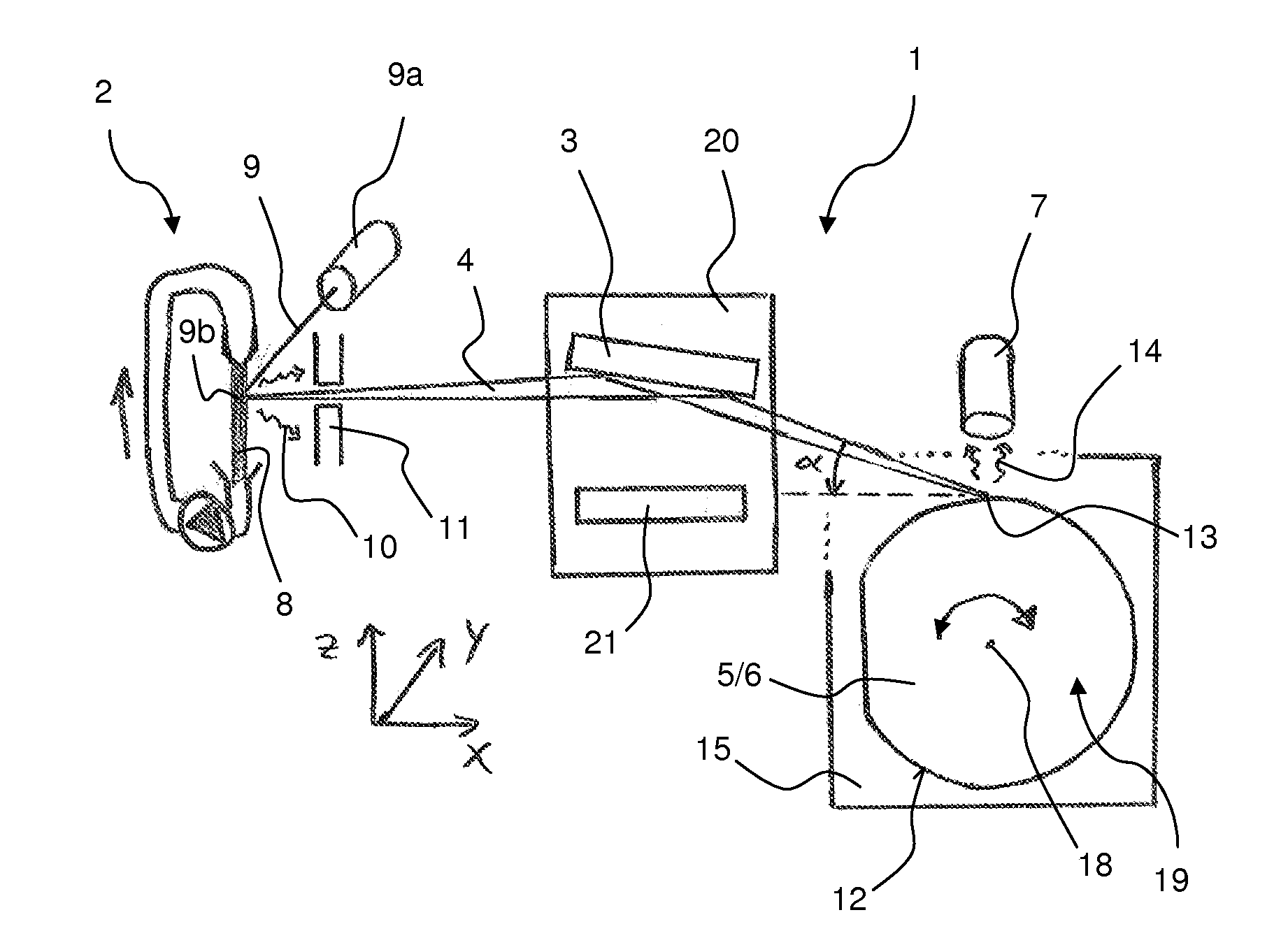
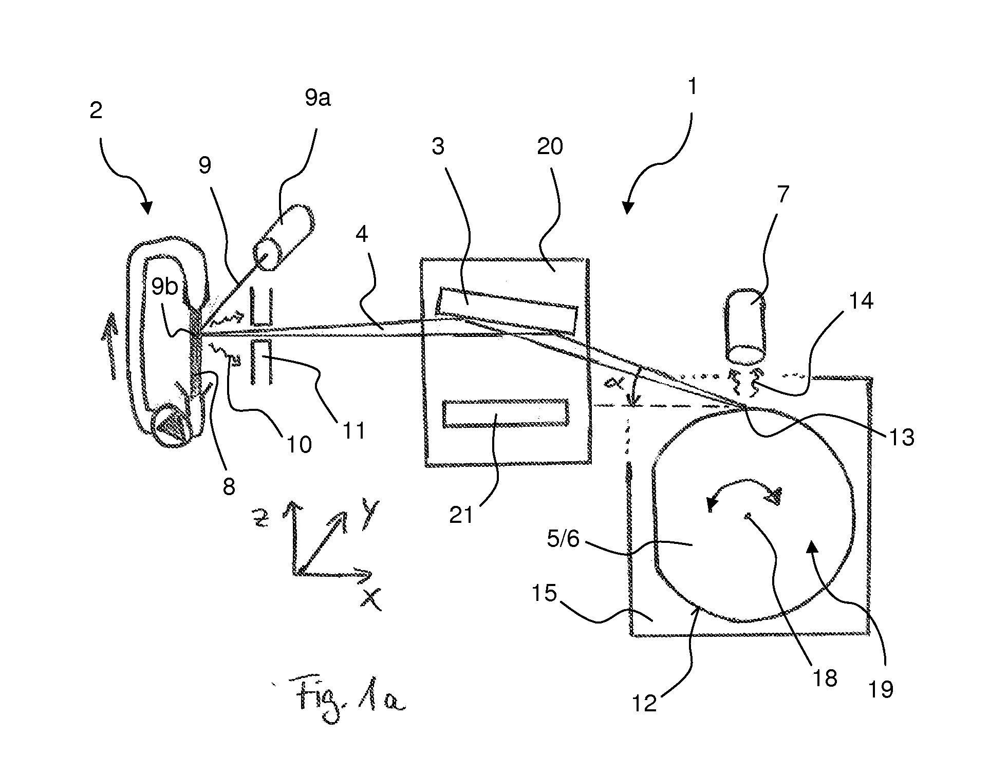
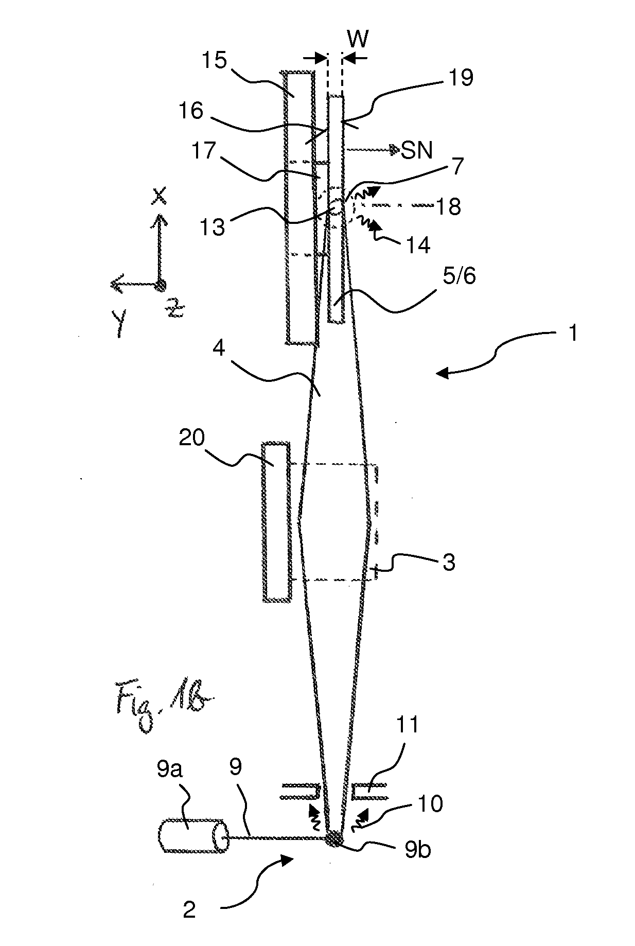
[0045]FIGS. 1a and 1b illustrate an embodiment of an inventive XRF measurement apparatus 1 by way of example, in a side view (FIG. 1a) and a top view (FIG. 1b).

[0046]The apparatus 1 comprises an x-ray source 2, x-ray optics 3 directing x-rays 4 from the x-ray source 2 to a sample 5, which is a disc shaped wafer 6, and an EDS detector 7.

[0047]The x-ray source 2 is, in the illustrated embodiment, of metal jet type, with a jet of liquid metal 8, for example slightly heated gallium, being hit by an electron beam 9 at a focal spot 9b. The electron beam 9 is generated by an electron beam source 9a; note that the electron beam 9 and metal jet 8 preferably propagate in vacuum. At the focal spot 9b of the electron beam 9, characteristic x-rays 10 and Bremsstrahlung are emitted. A fraction of the generated x-rays which passes an aperture 11 and is used as x-rays 4 (or primary beam) in the subsequent experimental setup. The brilliance of the x-ray source 2 together with the x-ray optics 3 is h...


PUM

PropertyMeasurementUnit
angleaaaaaaaaaa
angleaaaaaaaaaa
thicknessaaaaaaaaaa

Abstract

An XRF (XRF=x-ray fluorescence) measurement apparatus (1) has an x-ray source (2) for generating x-rays (4), x-ray optics (3) for directing x-rays (4) from the x-ray source (2) to a sample (5) and an EDS (EDS=energy dispersive spectroscopy) detector (7) for detecting fluorescent x-rays (14) from the sample (5). The apparatus is characterized in that the sample (5) is a wafer (6), in particular a Si wafer, wherein the x-ray optics (3) is positioned to direct the x-rays (4) onto the bevel (12) of the wafer (6). The x-ray source (2) plus the x-ray optics (3) has a brilliance of at least 5*107 counts / sec mm2, preferably at least 1*108counts / sec mm2. The apparatus allows an improved contamination control of wafers, in particular silicon wafers.

Description

[0001]This application claims Paris convention priority from EP 13 153 344.0 filed Jan. 30, 2013, the entire disclosure of which is hereby incorporated by reference.BACKGROUND OF THE INVENTION[0002]The invention relates to an XRF (XRF=x-ray fluorescence) measurement apparatus, comprising[0003]an x-ray source for generating x-rays,[0004]x-ray optics for directing x-rays from the x-ray source to a sample,[0005]the sample,[0006]and an EDS (EDS=energy dispersive spectroscopy) detector for detecting fluorescent x-rays from the sample.[0007]Such an XRF measurement apparatus is known from U.S. Pat. No. 5,778,039 A.[0008]Wafers, in particular silicon wafers, are a basic component in the production of semiconductor electronics. These semiconductor electronics are based on pn-transitions, in particular in diodes and transistors. Semiconductor material of p-type and n-type is produced by carefully controlling the chemical composition of a basic material (such as silicon). More specifically, do...

Claims


Application Information

Patent Timeline
Patent Type & Authority Applications(United States)
IPC IPC(8): G01N23/223
CPCG01N2223/6116G01N2223/076G01N23/223G01N2223/652G01N21/9501G01N21/9503G01N23/20025
Inventor VIGLIANTE, ASSUNTA
Owner BRUKER AXS
Why Eureka
Try Eureka