Method of manufacturing a magnetoresistive device

a technology of magnetoresistive device and manufacturing method, which is applied in the manufacture/treatment of galvano-magnetic device, basic electric element, electric apparatus, etc., can solve the problems of hard mask of photoresist and tetra-ethyl-ortho-silane (teos) that does not perform well under these two etches, change in bit shape, irregular bit shape, etc., to achieve high bit pattern fidelity, high aspect ratio, high high pattern fidelity ratio ratio ratio ratio ratio ratio ratio ratio ratio ratio ratio ratio ratio ratio ratio ratio ratio ratio ratio ratio ratio ratio ratio ratio ratio ratio ratio ratio ratio ratio ratio ratio ratio ratio ratio ratio ratio ratio ratio ratio ratio

Inactive Publication Date: 2014-07-31
EVERSPIN TECHNOLOGIES
View PDF7 Cites 4 Cited by
  • Summary
  • Abstract
  • Description
  • Claims
  • Application Information

AI Technical Summary

Benefits of technology

[0007]A method of manufacturing a magnetoresistive-based device provides high bit pattern fidelity by providing structures having a high aspect ratio and high pattern fidelity.

Problems solved by technology

A hard mask of photoresist and tetra-ethyl-ortho-silane (TEOS) does not perform well under these two etches.
This change in bit shape may be reduced by the use of a thick photoresist for high aspect ratio bits, but the thick photoresist has a tendency to collapse causing irregular bit shape.

Method used


Image

  • Method of manufacturing a magnetoresistive device
  • Method of manufacturing a magnetoresistive device
  • Method of manufacturing a magnetoresistive device

Examples


Embodiment Construction

[0014]The following detailed description is merely illustrative in nature and is not intended to limit the embodiments of the subject matter or the application and uses of such embodiments. Any implementation described herein as exemplary is not necessarily to be construed as preferred or advantageous over other implementations. Furthermore, there is no intention to be bound by any expressed or implied theory presented in the preceding technical field, background, brief summary, or the following detailed description.

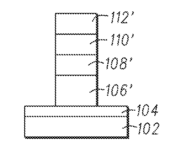
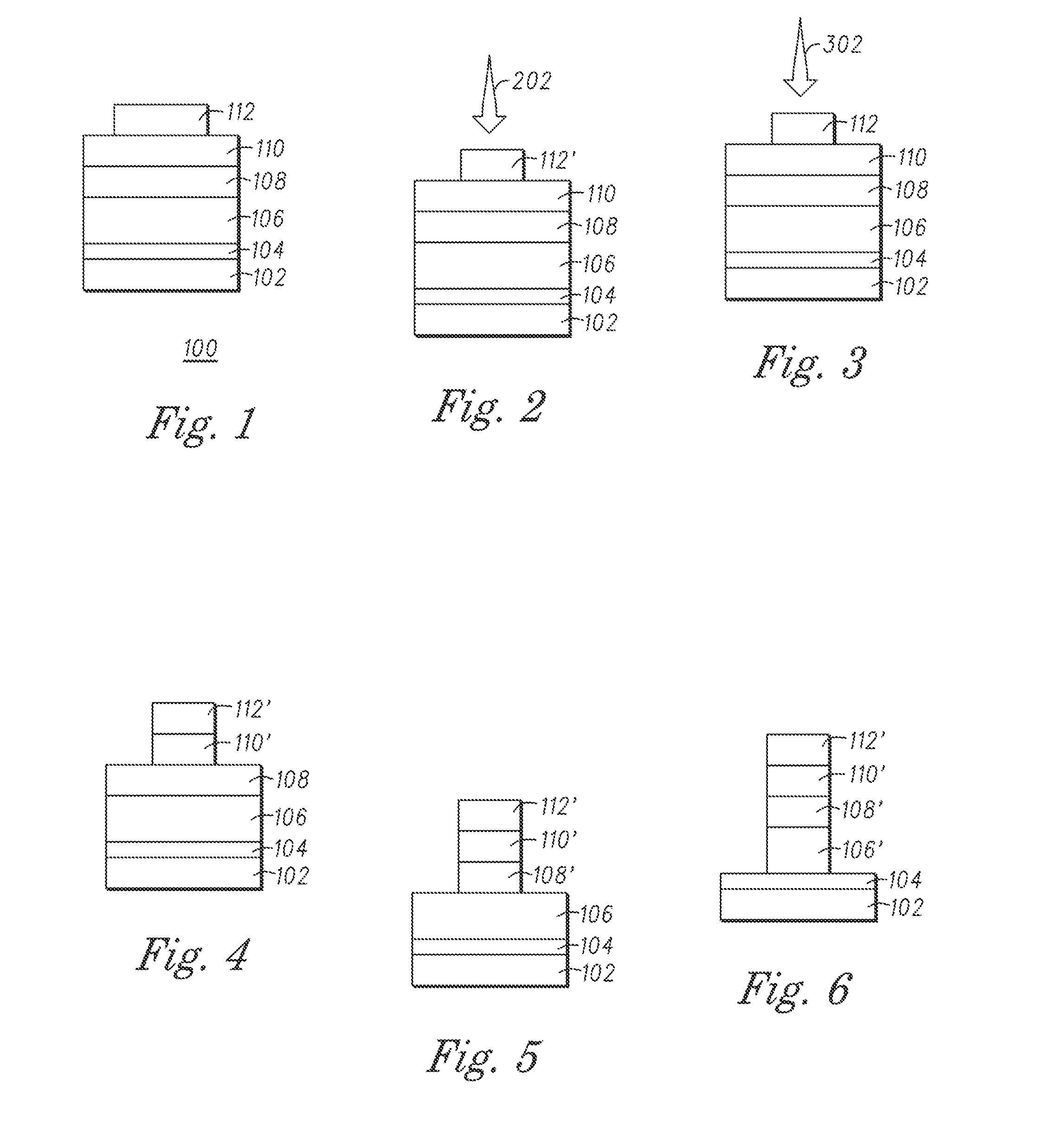
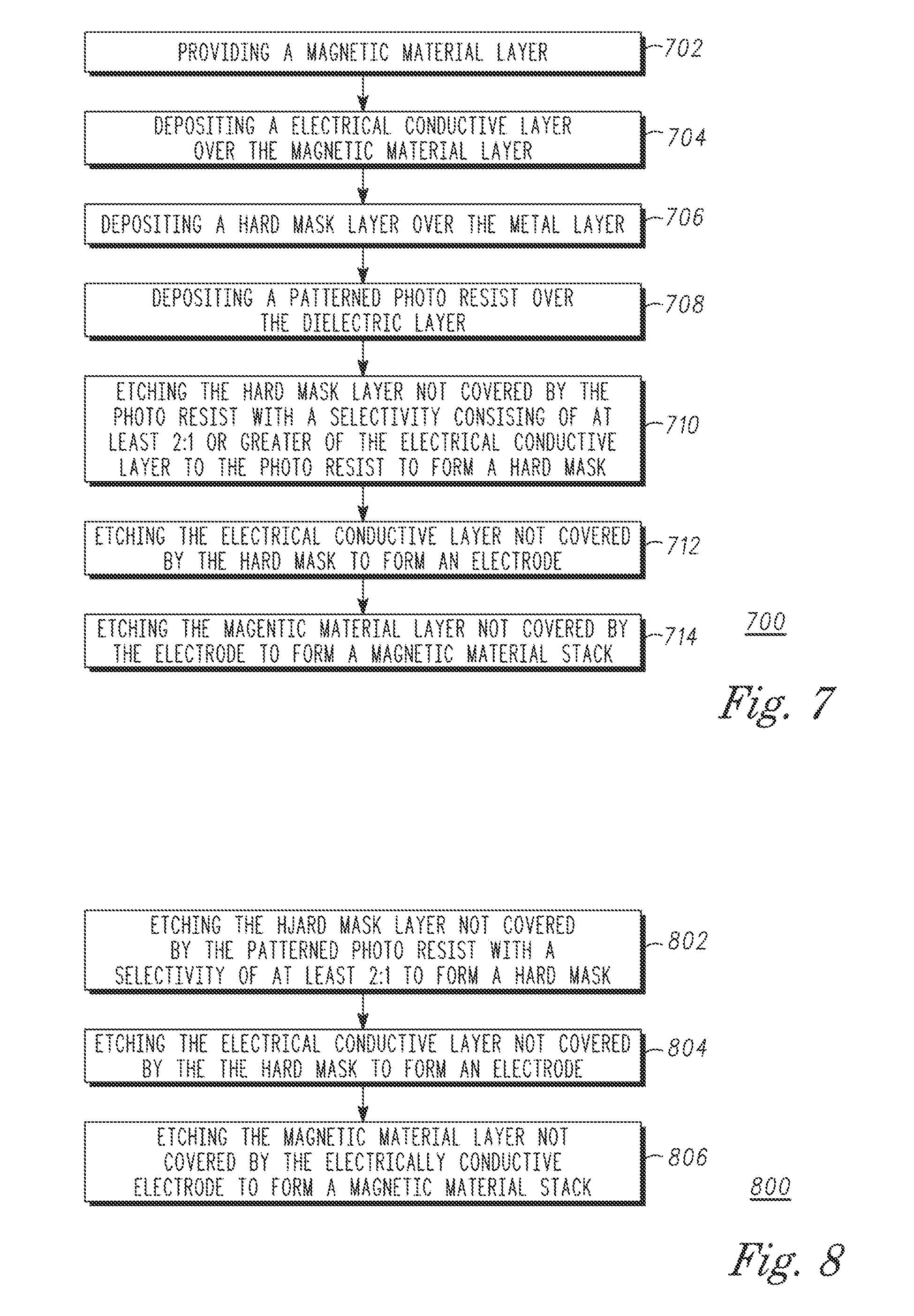
[0015]During the course of this description, like numbers are used to identify like elements according to the different figures that illustrate the various exemplary embodiments.

[0016]The exemplary embodiments described herein may be fabricated using known lithographic processes as follows. The fabrication of integrated circuits involves the creation of several layers of materials that interact in some fashion. One or more of these layers may be patterned so various regi...


PUM


Abstract

A method of manufacturing a magnetoresistive-based device includes etching a hard mask layer, the etching having a selectivity greater than 2:1 and preferably less than 5:1 of the hard mask layer to a photo resist thereover. Optionally, the photo resist is trimmed prior to the etch, and oxygen may be applied during or just subsequent to the trim of the photo resist to increase side shrinkage. An additional step includes an oxygen treatment during the etch to remove polymer from the structure and etch chamber.

Description

[0001]This application claims the benefit of U.S. Provisional Application No. 61 / 759,004 filed 31 Jan. 2013, which is incorporated herein by reference.TECHNICAL FIELD[0002]The exemplary embodiments described herein generally relates to methods of manufacturing an integrated circuit device, and more particularly to methods of manufacturing a magnetoresistive-based device, including etching techniques providing smaller structures / bits.BACKGROUND[0003]Magnetoelectronic devices, spin electronic devices, and spintronic devices are synonymous terms for devices that make use of effects predominantly caused by electron spin. Magnetoelectronics are used in numerous information devices to provide non-volatile, reliable, radiation resistant, and high-density data storage and retrieval. The numerous magnetoelectronic information devices include, but are not limited to, Magnetoresistive Random Access Memory (MRAM), magnetic sensors, and read / write heads for disk drives.[0004]Typically an MRAM in...

Claims


Application Information

Patent Timeline
Patent Type & Authority Applications(United States)
IPC IPC(8): H01L43/12
CPCH01L43/12H10N50/01
Inventor DESHPANDE, SARIN A.AGGARWAL, SANJEEV
Owner EVERSPIN TECHNOLOGIES
Why Eureka
Try Eureka