In situ silicon surface pre-clean for high performance passivation of silicon solar cells

a solar cell and silicon surface technology, applied in the field of photovoltaic device fabrication, can solve the problems of reducing the efficiency of the solar cell, and undesirable electrical short circuit of the shunt curren

Inactive Publication Date: 2014-07-31
APPLIED MATERIALS INC
View PDF5 Cites 17 Cited by
  • Summary
  • Abstract
  • Description
  • Claims
  • Application Information

AI Technical Summary

Benefits of technology

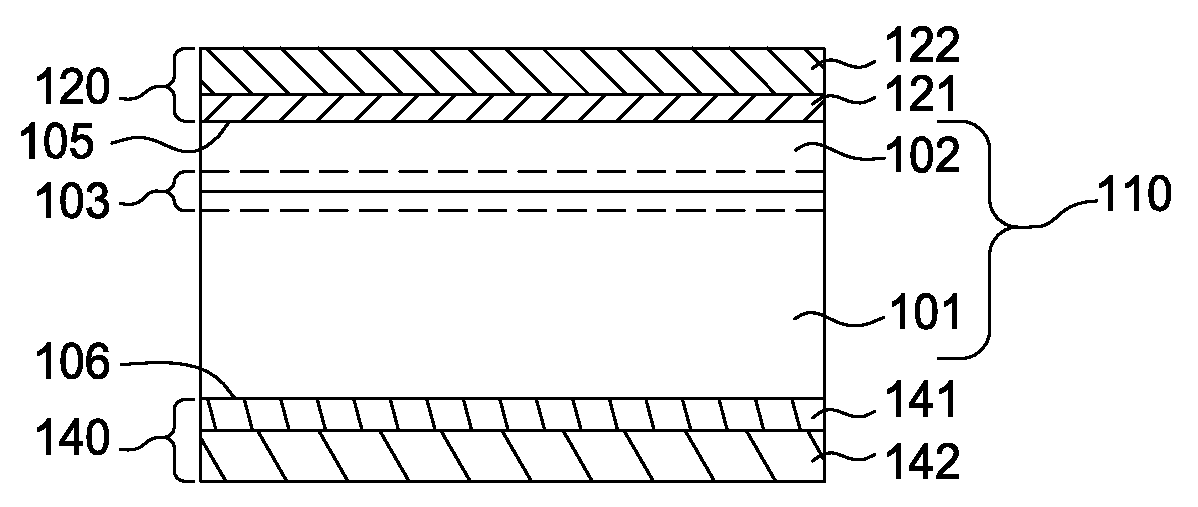
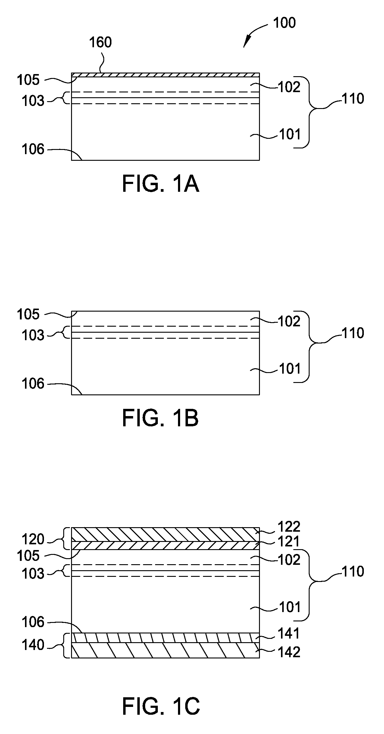
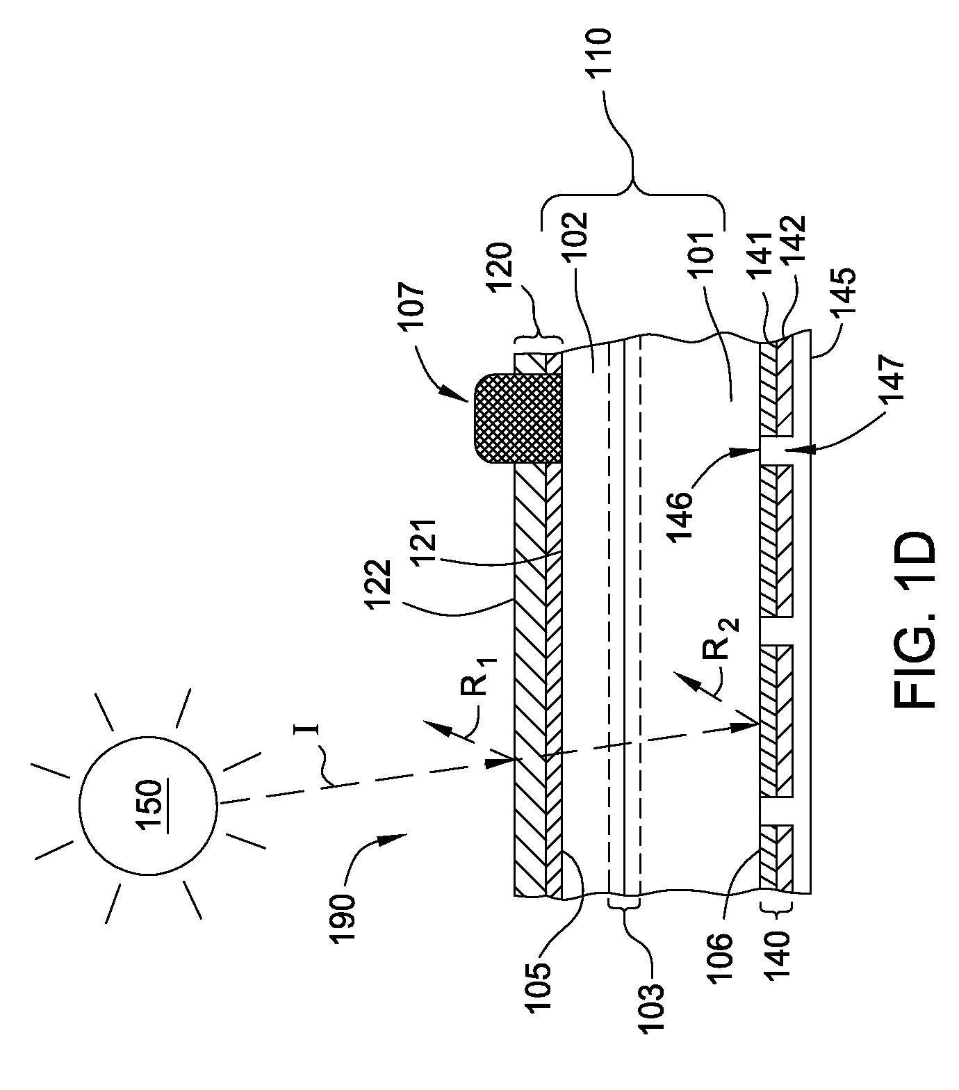
[0011]Embodiments of the invention generally relate to methods for fabricating photovoltaic devices, and more particularly to methods for in-situ cleaning of a solar cell substrates. In one embodiment, a method of manufacturing a solar cell device is provided. The method comprises exposing a single or poly crystalline silicon substrate to a wet clean process to clean the surfaces of the crystalline substrate, loading the crystalline silicon substrate into a processing system having a vacuum environment, exposing at least one surface of the crystalline silicon substrate to an in-situ cleaning process in the vacuum environment of the processing system, and forming one or more passivation layers on at least one surface of the crystalline silicon substrate in the processing system.
[0012]In another embodiment, a method of manufacturing a solar cell device is provided. The method comprises loading a crystalline silicon substrate into a processing system having a vacuum environment, exposing the crystalline silicon substrate to a hydrogen containing plasma in the vacuum environment of the processing system, and forming one or more passivation layers on at least one surface of the crystalline silicon substrate in the processing system.

Problems solved by technology

The efficiency at which a solar cell converts incident light energy into electrical energy is adversely affected by a number of factors.
Each time an electron-hole pair recombines, a charge carrier is eliminated, thereby reducing the efficiency of the solar cell.
Shunt current is an undesirable electrical short circuit between the front and back surface contacts of the solar cell.
However, after loading the crystalline silicon substrates into passivation layer deposition tools, surfaces of the crystalline silicon substrates may still be contaminated due to various reasons, for example, the presence of organic contaminants within processing chambers.

Method used


Image

  • In situ silicon surface pre-clean for high performance passivation of silicon solar cells
  • In situ silicon surface pre-clean for high performance passivation of silicon solar cells
  • In situ silicon surface pre-clean for high performance passivation of silicon solar cells

Examples


examples

[0065]The following non-limiting examples are provided to further illustrate embodiments described herein. However, examples are not intended to be all inclusive and are not intended to limit the scope of the embodiments described herein.

[0066]Samples #1-3 were performed on p-type CZ silicon bare wafers in an AKT-5500 PECVD chamber available from Applied Materials. The bare wafers were exposed to a hot-pass process to expose the wafers to possible residual contaminants present in the PECVD chamber. The hot-pass process may be performed with or without lamp heating. Exemplary hot-pass processes include: pre-processing chambers PH2, 330: 20% lamp power, heaters at 650° C.; AlO processing chamber, 340: heaters at 650° C.; transfer chamber PH3, 350: 20% lamp power, heaters at room temperature; SiN processing chamber, 360: heaters at 700° C. The hot-pass process was performed without deposition and without exposure to plasma to monitor the chamber environment. After exposure to the hot-p...


PUM

PropertyMeasurementUnit
temperaturesaaaaaaaaaa
temperatureaaaaaaaaaa

Abstract

Embodiments of the invention generally relate to methods for fabricating photovoltaic devices, and more particularly to methods for in-situ cleaning of a solar cell substrates. In one embodiment, a method of manufacturing a solar cell device is provided. The method comprises exposing a single or poly crystalline silicon substrate to a wet clean process to clean the surfaces of the crystalline substrate, loading the crystalline silicon substrate into a processing system having a vacuum environment, exposing at least one surface of the crystalline silicon substrate to an in-situ cleaning process in the vacuum environment of the processing system, and forming one or more passivation layers on at least one surface of the crystalline silicon substrate in the processing system.

Description

CROSS-REFERENCE TO RELATED APPLICATIONS[0001]This application claims benefit of U.S. Provisional Patent Application Ser. No. 61 / 758,542, filed Jan. 30, 2013 which is herein incorporated by reference in its entirety.BACKGROUND[0002]1. Field[0003]Embodiments of the invention generally relate to methods for fabricating photovoltaic devices, and more particularly to methods for in-situ cleaning of a solar cell substrates.[0004]2. Description of the Related Art[0005]Solar cells are photovoltaic devices that convert sunlight directly into electrical power. The most common material utilized in a solar cell is silicon, which is generally in the form of single crystalline silicon, polycrystalline silicon, or amorphous silicon. The ratio of light converted into electrical power versus the amount of light shined on the front or light-receiving surface of the solar cell is a measurement of the efficiency of the solar cell. Improvements in fabricating techniques undertake the task of increasing ...

Claims


Application Information

Patent Timeline
Patent Type & Authority Applications(United States)
IPC IPC(8): H01L31/18
CPCH01L31/1804H01L31/182H01L31/1864H01L31/1868H01L31/02167H01L31/056Y02E10/52Y02E10/546Y02E10/547Y02P70/50
Inventor SHENG, SHURANZHANG, LINPONNEKANTI, HARI K.
Owner APPLIED MATERIALS INC
Why Eureka
Try Eureka