Apparatus For Design-Based Manufacturing Optimization In Semiconductor Fab

a technology for optimizing semiconductor manufacturing and semiconductor fabs, applied in semiconductor/solid-state device testing/measurement, instruments, data processing applications, etc., can solve the problems of high production costs, high manufacturing environment, and high cost-intensive manufacturing environment for producing semiconductors, and achieve high scalable and secure, efficient semiconductor fab operation

Inactive Publication Date: 2014-07-31
APPLIED MATERIALS INC
View PDF14 Cites 5 Cited by
  • Summary
  • Abstract
  • Description
  • Claims
  • Application Information

AI Technical Summary

Benefits of technology

[0009]The present invention has been made to meet the above mentioned need and challenges in advanced semiconductor manufacturing. Accordingly, the present invention provides a fault-tolerant, highly scalable and secure server that focuses on the complex inter-dependency of device design and manufacturing for achieving efficient semiconductor fab operation.

Problems solved by technology

Producing semiconductors requires a very cost-intensive and sophisticated manufacturing environment.
With the size of the structures built on a semiconductor chip decreasing, the production costs are increasing at the same pace.
The process of integrated circuit (IC) manufacturing often requires hundreds of sequential steps, each one of which could lead to yield loss.
Consequently, maintaining product quality in a semiconductor manufacturing facility often requires the strict control of hundreds or even thousands of process variables.
However, huge amount of data are generated each day from hundreds of equipments, it is difficult to extract hidden relationships between numerous complex process control parameters.
As the advanced semiconductor technology pushes the physics limits to shrink the size of the device, there is ever-increasing inter-dependency between device design and device manufacturing process.
However, the inter-dependency has rarely been utilized to optimize the semiconductor manufacturing process because of the availability of the device design data and the security concern in exposing the device design data in the manicuring flow of the semiconductor process.

Method used


Image

  • Apparatus For Design-Based Manufacturing Optimization In Semiconductor Fab
  • Apparatus For Design-Based Manufacturing Optimization In Semiconductor Fab
  • Apparatus For Design-Based Manufacturing Optimization In Semiconductor Fab

Examples


Embodiment Construction

[0022]The accompanying drawings are included to provide a further understanding of the invention, and are incorporated in and constitute a part of this specification. The drawing illustrates embodiments of the invention and, together with the description, serves to explain the principles of the invention.

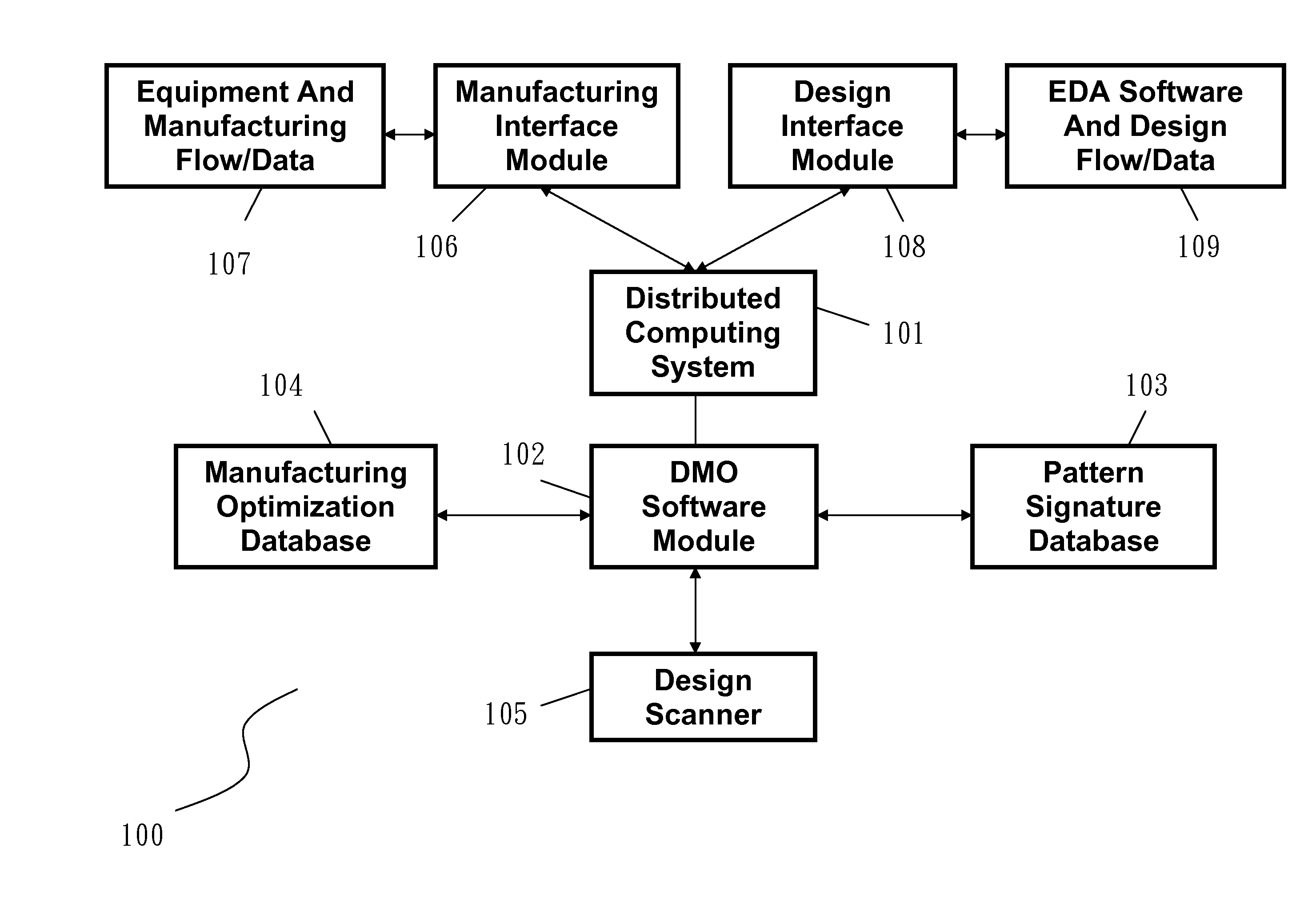
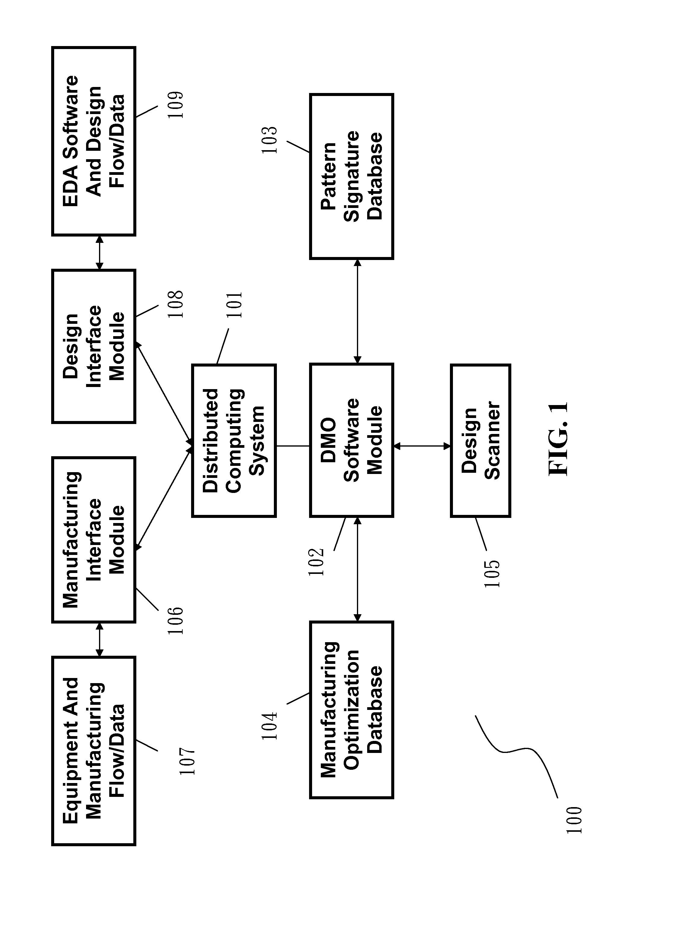
[0023]FIG. 1 shows a block diagram of the integrated design-based manufacturing optimization (DMO) server 100 according to the present invention. The DMO server 100 comprises a distributed computing system 101 and a DMO software module 102. The DMO server 100 further has a pattern signature database 103 and a manufacturing optimization database 104 and a designer scanner 105. The distributed computing system 101 is connected to a design interface module 108 to communicate with EDA software and design flow 109, and a manufacturing interface module 106 to communicate with equipment and manufacturing flow 107.

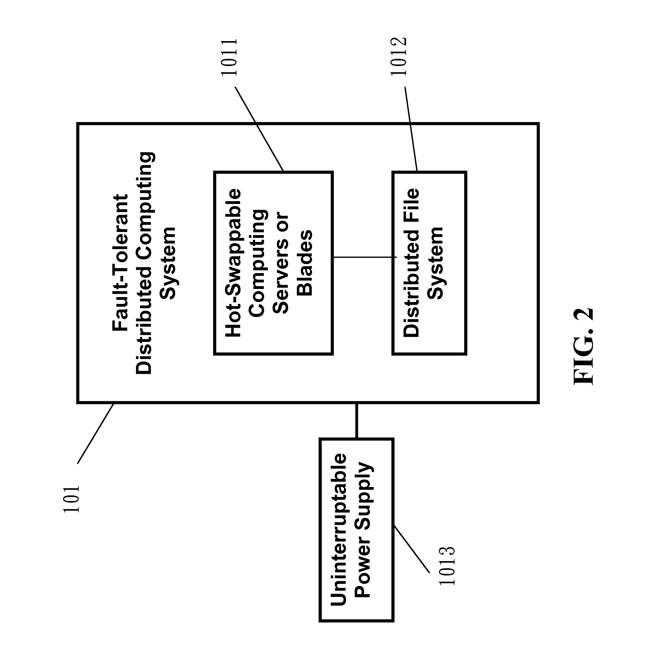
[0024]As shown in FIG. 2, the distributed computing system 101 is a fault-tol...


PUM


Abstract

A design-based manufacturing optimization (DMO) server comprises a distributed computing system and a DMO software module incorporating with a design scanner to scan and analyze design data of a semiconductor device for optimizing manufacturing of the semiconductor device. The DMO software module sets up a pattern signature database and a manufacturing optimization database, generates design-based manufacturing recipes, interfaces with manufacturing equipment through a manufacturing interface module, and interfaces with electronic design automation suppliers for the design data through a design interface module. The DMO server executes the design-based manufacturing recipes for manufacturing optimization.

Description

BACKGROUND OF THE INVENTION[0001]1. Field of the Invention[0002]The present invention relates generally to semiconductor manufacturing, and more particularly to an apparatus for optimizing semiconductor manufacturing based on design.[0003]2. Description of Related Arts[0004]Producing semiconductors requires a very cost-intensive and sophisticated manufacturing environment. With the size of the structures built on a semiconductor chip decreasing, the production costs are increasing at the same pace. Semiconductor production in a modern fab requires several hundreds of machines, with prices reaching several ten-millions or even hundred-millions of US dollars per machine.[0005]The process of integrated circuit (IC) manufacturing often requires hundreds of sequential steps, each one of which could lead to yield loss. Consequently, maintaining product quality in a semiconductor manufacturing facility often requires the strict control of hundreds or even thousands of process variables. Th...

Claims


Application Information

Patent Timeline
Patent Type & Authority Applications(United States)
IPC IPC(8): G06Q10/06
CPCH01L22/12H01L22/20
Inventor JUANG, SHAUH-TEHLIN, JASON ZSE-CHERNG
Owner APPLIED MATERIALS INC
Why Eureka
Try Eureka