

Photovoltaic Device Including a P-N Junction and Method of Manufacturing
- Summary
- Abstract
- Description
- Claims
- Application Information
AI Technical Summary
Benefits of technology
Problems solved by technology
Method used
Image

Examples
first embodiment
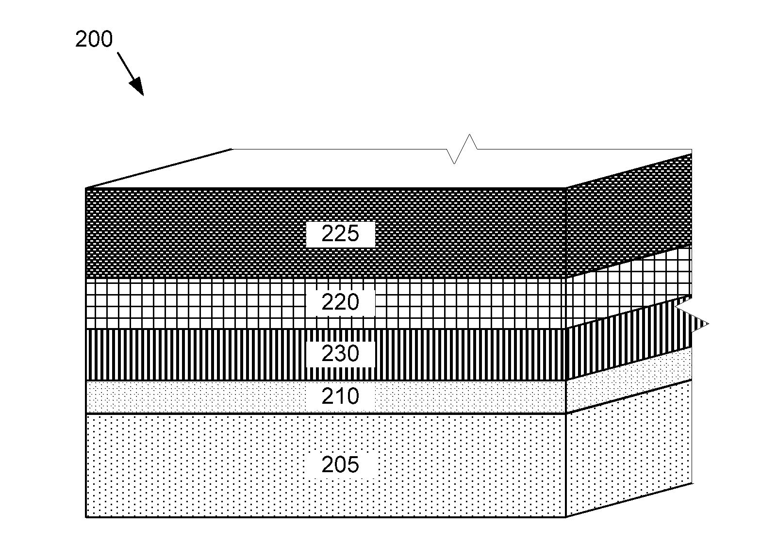
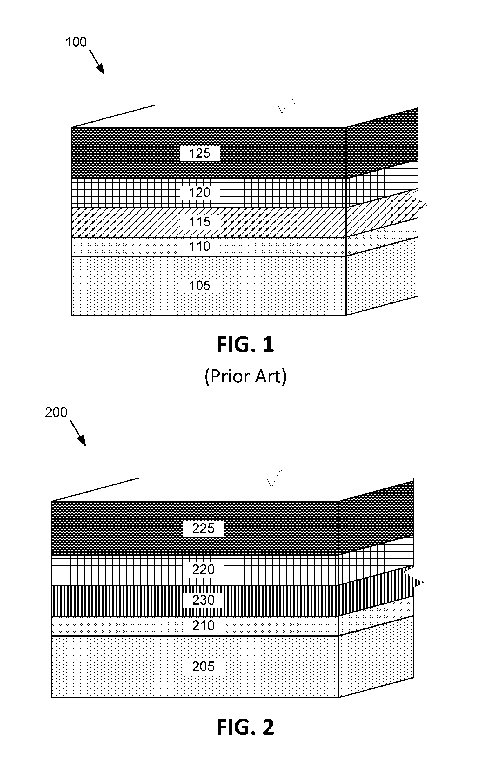
[0029]Several specific embodiments of a novel photovoltaic device will be described with reference to the figures. The novel photovoltaic device according to the disclosed embodiments can include material compositions, or interfacial layers to achieve high performance efficiency in the p-n junction. In a photovoltaic device 200 according to the present disclosure as depicted in FIG. 2, an n-type window layer 230 comprising cadmium sulphoselenide (CdSSe) is deposited over a substrate structure including a base layer 205 and a TCO layer 210. A p-type absorber layer 220 is deposited over the CdSSe layer 230. The CdSSe layer 230 and the p-type absorber layer 220 form a p-n junction in the photovoltaic device 200. A metal back contact 225 is formed over the p-type absorber layer 220.
[0030]The base layer 205 may include glass, for example, soda lime glass or float glass. Alternatively, the base layer 205 may include polymeric, ceramic, or other materials that provide a suitable structure ...
third embodiment
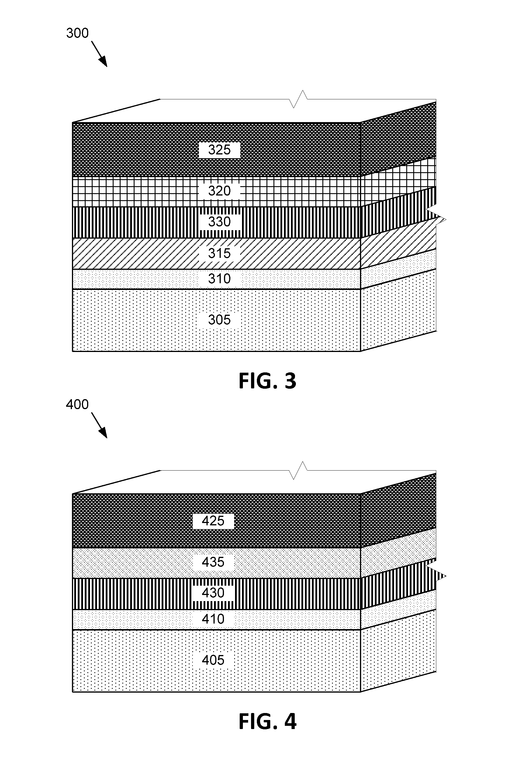
[0039]In a photovoltaic device 400, as depicted in FIG. 4, an n-type CdSSe window layer 430 is deposited over a substrate structure including a base layer 405 and a TCO layer 410. A cadmium sulphotelluride (CST) p-type absorber layer 435 is deposited over the CdSSe layer 430. A metal back contact 425 is formed over the p-type CST absorber layer 435. The CST absorber layer 435 may be composed of cadmium sulfur and tellurium in varying amounts to form a CdSxTe1−x compound, where x may be between 1 to 30 at %, or alternatively between 1 to 15 at %, or further alternatively between 2 to 10 at %. A CST absorber layer 435 may be between 500 to 8000 nm thick, or alternatively between 1000 nm to 3500 nm thick. A CST layer may be formed by a deposition process, such as vapor transport deposition, atomic layer deposition, chemical bath deposition, sputtering, closed space sublimation, or any other suitable process.
fourth embodiment
[0040]In a photovoltaic device 500, as depicted in FIG. 5, an n-type window layer of CdSSe 530 is deposited over a substrate structure including a base layer 505 and a TCO layer 510. A CST interfacial layer 535 is deposited over the n-type CdSSe window layer 530. A p-type CdTe absorber layer 520 is deposited over the CST interfacial layer 535. The CST interfacial layer 535 may be similarly composed of CdSxTe1−x, where x may be between 1 to 30 at %, or alternatively between 1 to 15 at %, or further alternatively between 2 to 10 at %. However, a CST interfacial layer 535 adjacent to the CdTe absorber layer 520 may be between 20 nm to 1000 nm thick, or alternatively may be between 400 nm to 600 nm thick. The CST interfacial layer 535 and the p-type CdTe absorber layer 520 together form the p-type region of the p-n junction with the n-type CdSSe window layer 530. A metal back contact 525 is formed over the p-type CdTe layer 520.
PUM
 Abstract
Description
Claims
Application Information