
Air-spacer mos transistor

Active Publication Date: 2014-08-07
STMICROELECTRONICS CROLLES 2 +2
View PDF21 Cites 18 Cited by
  • Summary
  • Abstract
  • Description
  • Claims
  • Application Information

AI Technical Summary

Benefits of technology

The patent describes a new design for a MOS transistor with a conductive gate stack that has a lower and an upper portion. The upper portion is shorter than the lower and is bordered with air or dielectric spacers. The lower portion has a layer of metal or metal alloy and a doped polysilicon layer, while the upper portion has a layer of doped polycrystalline silicon-germanium or silicon-germanium. A method is also provided for manufacturing this new design MOS transistor. The technical effects of this new design include improved performance and reliability.

Problems solved by technology

Indeed, in this case, the distances between the gate, on the one hand, and the source, the drain, the source contact, and the drain contact, on the other hand, become extremely small.

Method used


Image

  • Air-spacer mos transistor
  • Air-spacer mos transistor
  • Air-spacer mos transistor

Examples


Embodiment Construction

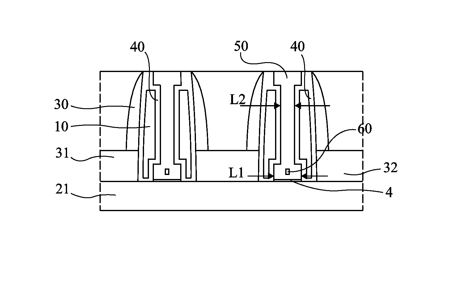
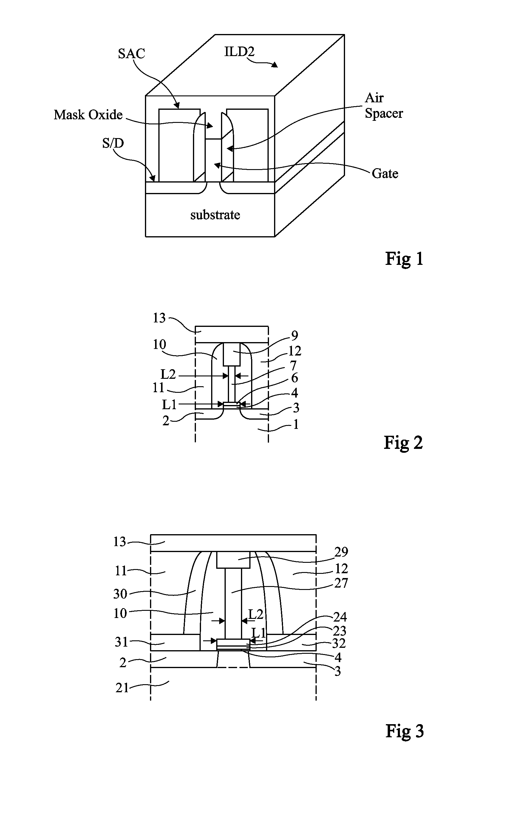
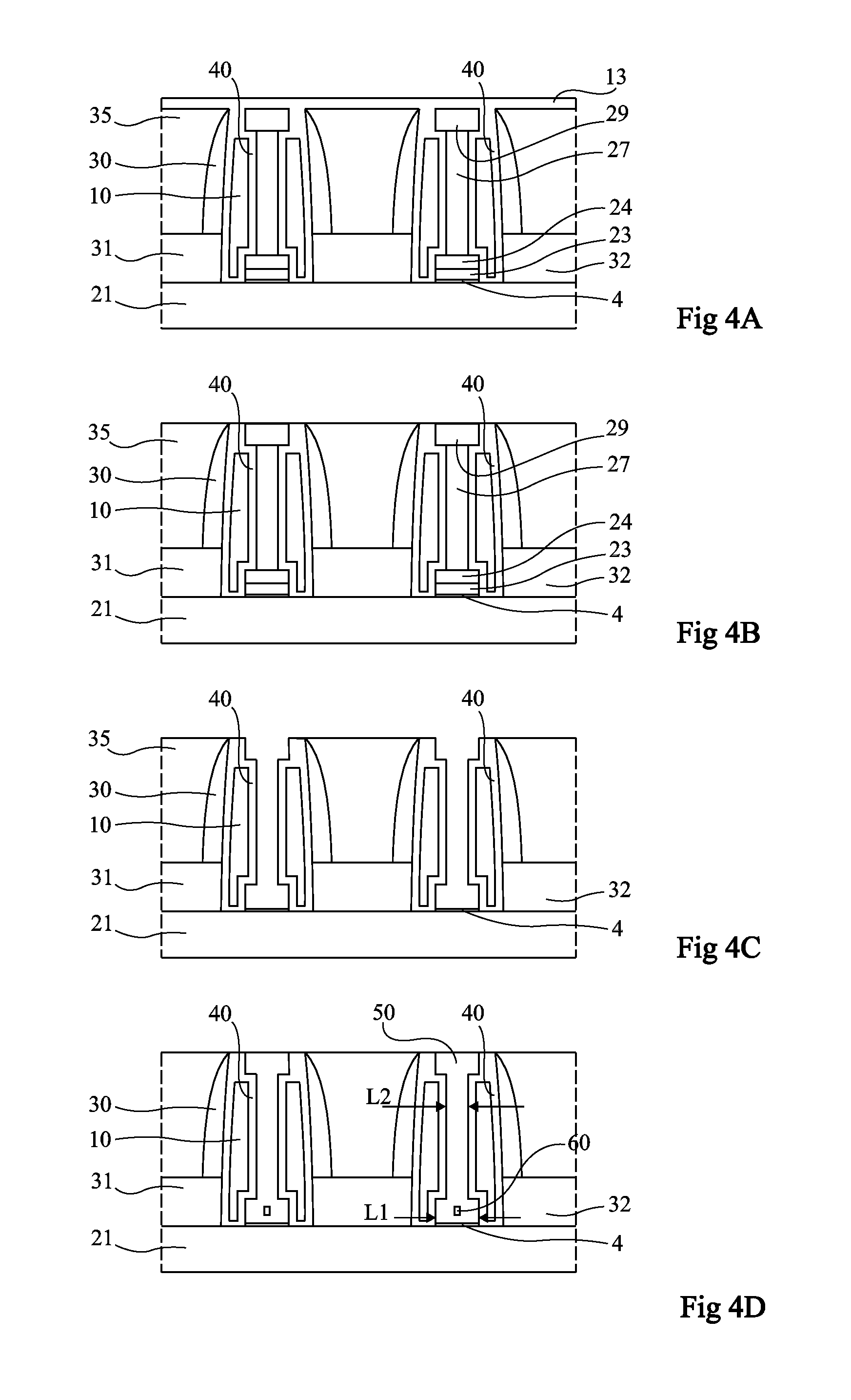
[0032]The use of air spacers has the advantage over the use of solid dielectric spacers that air (or vacuum) has a very low dielectric constant, close to 1, while the materials currently used in microelectronics for spacers, such as silicon oxide or silicon nitride, have dielectric constants higher than 2.5, or even 4. Further, it is generally desirable to decrease the size of spacers, on the one hand for the simplicity of their forming, on the other hand to reduce the size of components to which these spacers are associated.

[0033]As will be gathered from an analysis of the various documents describing air spacers, such spacers are obtained by first forming solid dielectric spacers, and by then removing these spacers by etching and closing the upper portion of the cavity thus formed. The general size of spacers is thus imposed by technology.

[0034]Further, the case where the transistor which is desired to be manufactured is a transistor of minimum size, that is, where the gate length...


PUM


Abstract

A MOS transistor including, above a gate insulator, a conductive gate stack having a height, a length, and a width, this stack having a lower portion close to the gate insulator and an upper portion, wherein the stack has a first length in its lower portion, and a second length shorter than the first length in its upper portion.

Description

CROSS REFERENCE TO RELATED APPLICATION[0001]This application claims priority to French Patent Application No. 13 / 50941, filed Feb. 4, 2013, which is hereby incorporated by reference to the maximum extent allowable by law.BACKGROUND[0002]1. Technical Field[0003]The present disclosure relates to MOS transistors, and more specifically to air-spacer MOS transistors.[0004]2. Discussion of the Related Art[0005]In the forming of a MOS transistor, it is generally desired to decrease the power consumption on switching and to increase the switching speed. Such parameters especially depend on the gate-source, gate-drain, gate-source contact, and gate-drain contact capacitances.[0006]Such stray capacitances tend to become particularly significant in the case of MOS transistors of very small size, where the gate lengths are shorter than some hundred nanometers, and especially shorter than 20 nm. Indeed, in this case, the distances between the gate, on the one hand, and the source, the drain, the...

Claims


Application Information

Patent Timeline
IPC IPC(8): H01L29/49H01L21/28
CPCH01L29/49H01L29/4925H01L21/28008H01L21/28114H01L29/42376H01L29/4991H01L29/6653H01L29/66545H01L29/6656H01L29/66628
Inventor NIEBOJEWSKI, HEIMANUMORAND, YVESLE ROYER, CYRILLE
Owner STMICROELECTRONICS CROLLES 2
Features
  • Generate Ideas
  • Intellectual Property
  • Life Sciences
  • Materials
  • Tech Scout
  • Unparalleled Data Quality
  • Higher Quality Content
  • 60% Fewer Hallucinations
Learn More