Semiconductor gate structure for threshold voltage modulation and method of making same

a technology of threshold voltage modulation and semiconductor gate structure, which is applied in the direction of semiconductor devices, basic electric elements, electrical appliances, etc., can solve the problems of non-uniformity, higher gate leakage, and reliability concerns, and achieve the effect of reducing the work function of the n-type transistor

Inactive Publication Date: 2014-08-21
GLOBALFOUNDRIES US INC
View PDF1 Cites 253 Cited by
  • Summary
  • Abstract
  • Description
  • Claims
  • Application Information

AI Technical Summary

Benefits of technology

[0006]The present invention provides, in a second aspect, further reducing a work function of the n-type transistor. The further reducing includes annealing to combine over the n-type transistor a layer of a fi

Problems solved by technology

However, there are reliability concerns and higher gate leakage with the use of such metals, mainly stemming from the relatively low controllability of aluminum diffusion.
Non-uniformity is also a concer

Method used


Image

  • Semiconductor gate structure for threshold voltage modulation and method of making same
  • Semiconductor gate structure for threshold voltage modulation and method of making same
  • Semiconductor gate structure for threshold voltage modulation and method of making same

Examples


Embodiment Construction

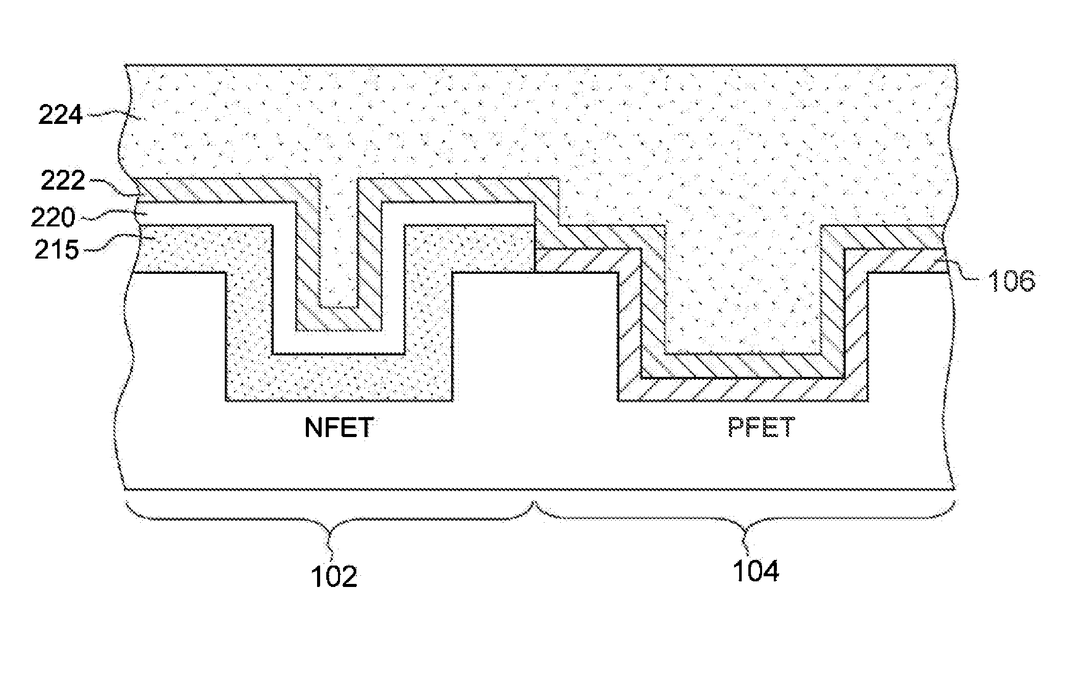
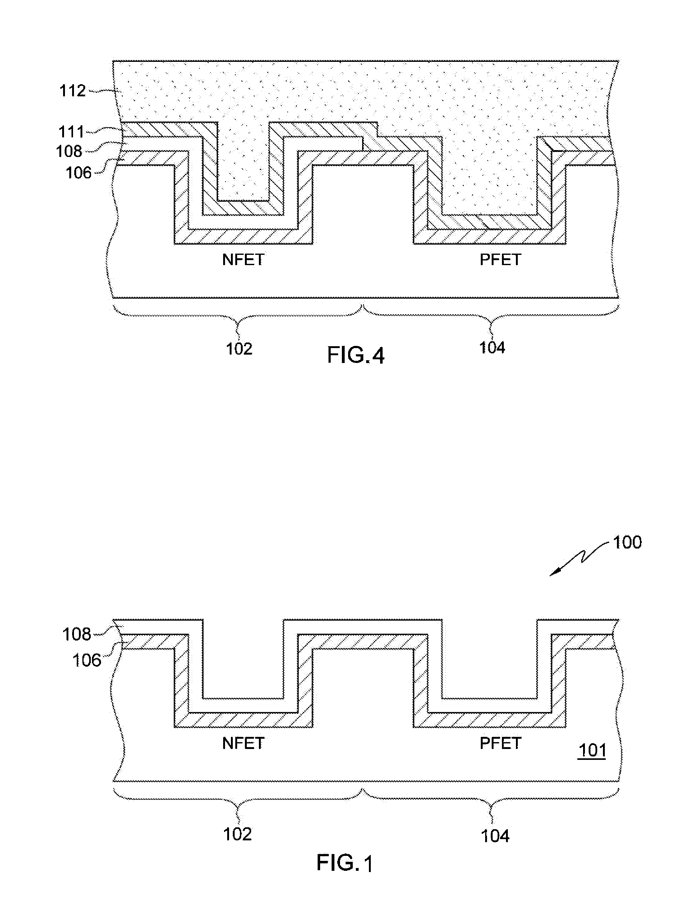
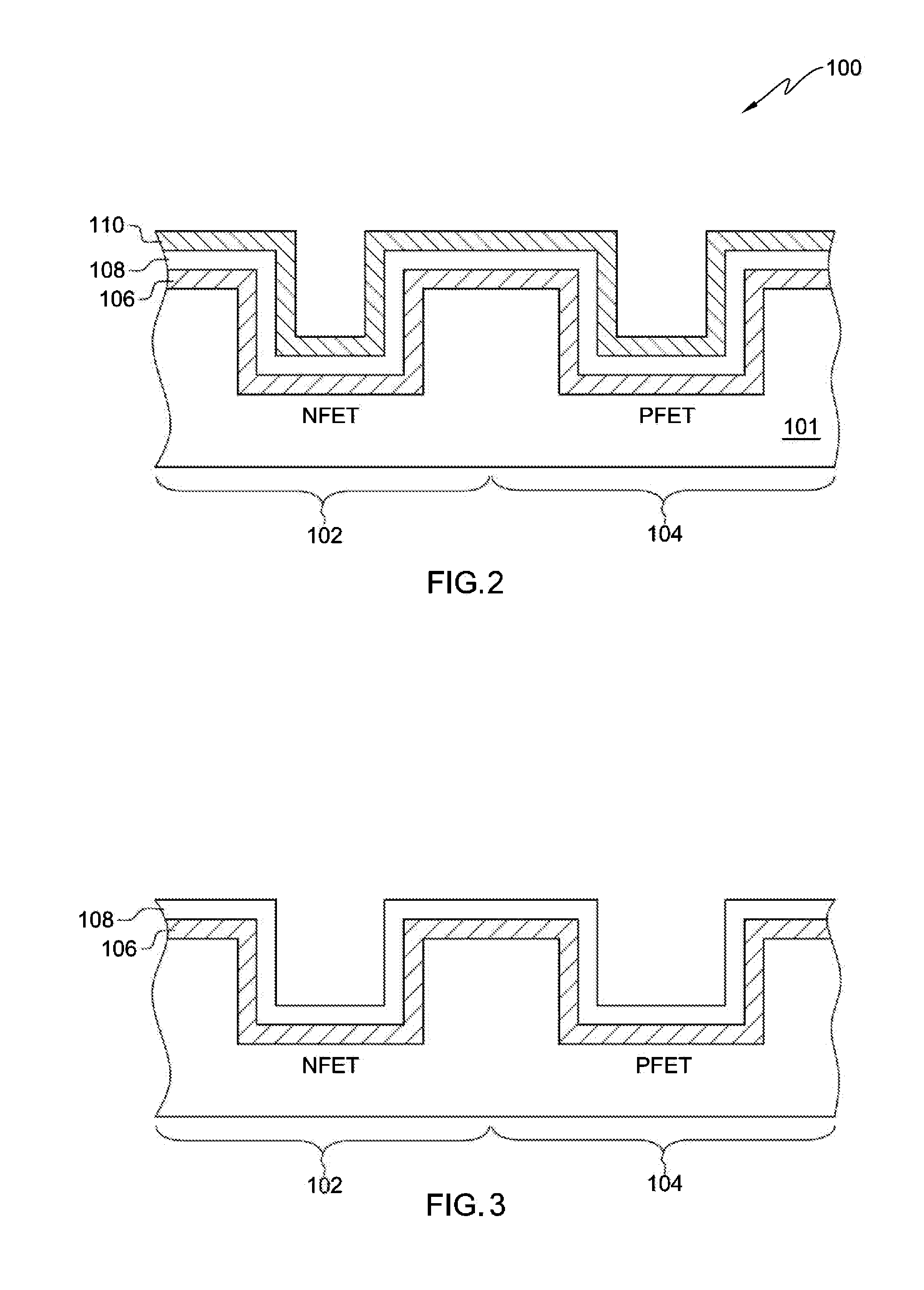
[0012]Aspects of the present invention and certain features, advantages, and details thereof, are explained more fully below with reference to the non-limiting examples illustrated in the accompanying drawings. Descriptions of well-known materials, fabrication tools, processing techniques, etc., are omitted so as not to unnecessarily obscure the invention in detail. It should be understood, however, that the detailed description and the specific examples, while indicating aspects of the invention, are given by way of illustration only, and are not by way of limitation. Various substitutions, modifications, additions, such as additional fabrication steps and / or additional layers of materials, and / or different arrangements of certain disclosed layers, within the spirit and / or scope of the underlying inventive concepts will be apparent to those skilled in the art from this disclosure.

[0013]Approximating language, as used herein throughout the specification and claims, may be applied to...


PUM


Abstract

A gate structure of a semiconductor device having a NFET and a PFET, includes a lower layer of a hafnium-based dielectric over the gates of the NFET and PFET, and an upper layer of a lanthanide dielectric. The dielectrics are annealed to mix them above the NFET resulting in a lowered work function, and corresponding threshold voltage reduction. An annealed, relatively thick titanium nitride cap over the mixed dielectric above the NFET gate also lowers the work function and threshold voltage. Above the TiN cap and the hafnium-based dielectric over the PFET gate, is another layer of titanium nitride that has not been annealed. A conducting layer of tungsten covers the structure.

Description

BACKGROUND OF THE INVENTION[0001]1. Technical Field[0002]The present invention generally relates to semiconductor devices and methods of fabricating the same. More particularly, the present invention relates to fabrication of a semiconductor gate structure for modulation of threshold voltage by selectively annealing a work function material lacking aluminum.[0003]2. Background Information[0004]Controlling the threshold voltage (i.e., minimum turn-on voltage, Vth) of a transistor is a long-standing goal of transistor design. Currently, aluminum containing n-type metals are used for Vth control by controlling the thickness of the aluminum containing n-type metals. However, there are reliability concerns and higher gate leakage with the use of such metals, mainly stemming from the relatively low controllability of aluminum diffusion. Non-uniformity is also a concern, due to poor aluminum diffusion distribution. In addition, many aluminum containing materials used for atomic layer depos...

Claims


Application Information

Patent Timeline
IPC IPC(8): H01L29/40H01L29/49
CPCH01L29/4966H01L29/401H01L21/28088H01L21/823842H01L29/513H01L29/517H01L29/40114
Inventor KIM, HOONCHOI, KISIK
Owner GLOBALFOUNDRIES US INC
Why Eureka
Try Eureka