
Solar cell unit and method for manufacturing the same

a solar cell and unit technology, applied in the field of solar cells, can solve the problems of weakened light adsorption efficiency inability to make solar cell units in the aforementioned structure fairly thin, and ineffective etc., to achieve the effect of improving photoelectric conversion efficiency, improving electrical current density of solar cell units, and effective collection of photogenic charge carriers

Inactive Publication Date: 2014-08-28
LUO ZHIJIONG +2
View PDF4 Cites 10 Cited by
  • Summary
  • Abstract
  • Description
  • Claims
  • Application Information

AI Technical Summary

Benefits of technology

The present invention is a solar cell unit and a method for manufacturing it that reduces the thickness of the semiconductor plate without compromising its performance. By reducing the thickness of the solar cell unit, the efficiency of the unit is improved, resulting in more solar cells per substrate and higher manufacturing yield. Additionally, the solar cell unit does not require the formation of electrodes on both sides, thereby improving the light absorption efficiency and conversion efficiency of the solar unit.

Problems solved by technology

The aforementioned structure puts constraint on the thickness of the solar cell unit; namely, the solar cell unit in aforementioned structure cannot be made fairly thin.
In the case the thickness of a solar cell unit is made fairly thin, in particular the thickness of the solar cell unit is close to or smaller than the width of depletion region, the light adsorption efficiency of the solar cell unit would be weakened, and the electrical current in the solar cell unit would become smaller when the thickness of the solar cell unit becomes thinner, which consequently curtails performance of the solar cell unit.
Thus, the utility of the semiconductor plate material cannot be further improved.
Particularly, it is impossible to increase the number of semiconductor plates, when the semiconductor plates are made out of a substrate.
However, the electrodes would block light and degrade energy conversion efficiency of the solar cell unit.

Method used


Image

  • Solar cell unit and method for manufacturing the same
  • Solar cell unit and method for manufacturing the same
  • Solar cell unit and method for manufacturing the same

Examples


Embodiment Construction

[0048]Embodiments of the present invention are to be described at length below, wherein examples of embodiments are illustrated in the appended drawings. It should be appreciated that embodiments described below in conjunction with the drawings are illustrative, and are provided for explaining the present invention only, thus shall not be interpreted as a limit to the present invention. Various embodiments or examples are provided here below to implement different structures of the present invention. To simplify the disclosure of the present invention, descriptions of components and arrangements of specific examples are given below. They are only illustrative and not intended to limit the present invention. Moreover, in the present invention, reference numbers and / or letters may be repeated in different examples. Such repetition is for purposes of simplicity and clarity, yet does not denote any relationship between respective embodiments and / or arrangements under discussion. Further...


PUM


Abstract

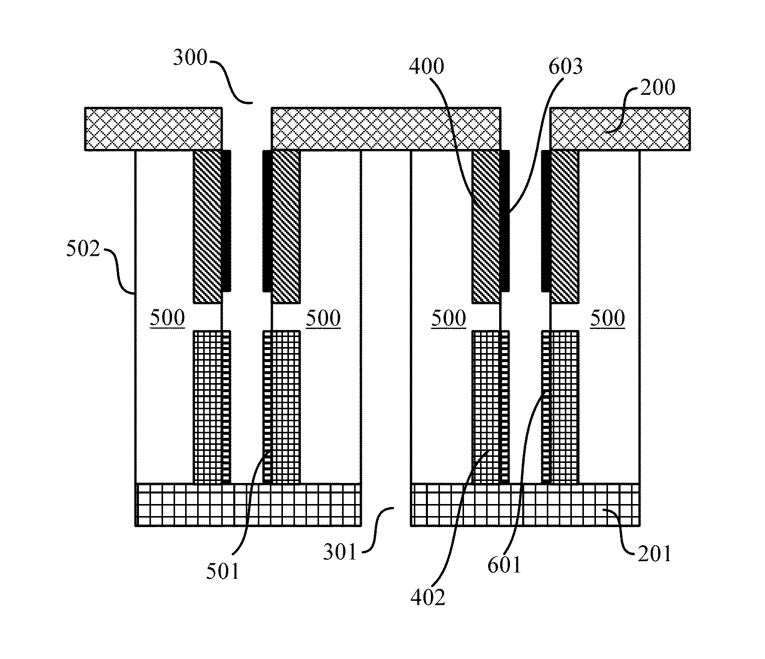
The present invention provides a solar cell unit, which comprises a semiconductor plate of first-type doping or second-type doping; wherein the semiconductor plate has a first surface and a second surface opposite to the first surface; the semiconductor plate comprises a first-type doping region and second-type doping region, both the first-type doping region and the second-type doping region are located on the first surface of the semiconductor plate; a first sheet is provided on the side surface of the semiconductor plate that is adjacent to the first-type doping region, and a second sheet is provided on the side surface of the semiconductor plate that is adjacent to the second type doping region.

Description

FIELD OF THE INVENTION[0001]The present invention relates to the technical filed of solar cells, particularly, to a solar cell unit and a method for manufacturing the same.BACKGROUND OF THE INVENTION[0002]Due to growing concern of energy shortage and environmental challenges, solar energy has been regarded as a potential solution. At the heart of the photovoltaic industry is a solar cell which converts photon energy to electrical energy. With rapid technological advancements in the photovoltaic industry, solar cells have been widely used in various applications. From the creation of solar cells, the technicians working in this technical field have devoted themselves to improve conversion efficiency of solar cells.[0003]As shown in FIG. 37, a solar cell unit in the prior art typically comprises a semiconductor plate 10 of p-type doped configuration or n-type doped configuration; a p+ doping region 20 is arranged on a primary surface of the semiconductor plate 10, while an n+ doping r...

Claims


Application Information

Patent Timeline
Patent Type & Authority Applications(United States)
IPC IPC(8): H01L31/18H01L31/04
CPCH01L31/1876H01L31/04H01L31/18H01L31/188H01L31/035281H01L31/042H01L31/0504H01L31/1804H01L31/202Y02E10/547Y02P70/50
Inventor LUO, ZHIJIONGZHU, HUILONGYIN, HAIZHOU
Owner LUO ZHIJIONG
Learn More