Method for manufacturing monolithic ceramic electronic component
a technology of monolithic ceramics and electronic components, applied in the direction of capacitor manufacturing, stacked capacitors, fixed capacitor details, etc., can solve the problems of easy peeling and structural defects of ceramic layers, and achieve the effect of significantly reducing or preventing peeling and structural defects
- Summary
- Abstract
- Description
- Claims
- Application Information
AI Technical Summary
Benefits of technology
Problems solved by technology
Method used
Image
Examples
experimental example 1
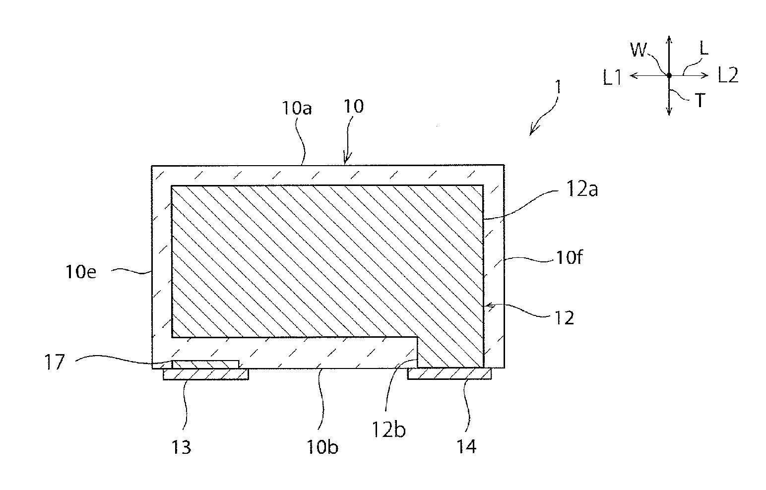
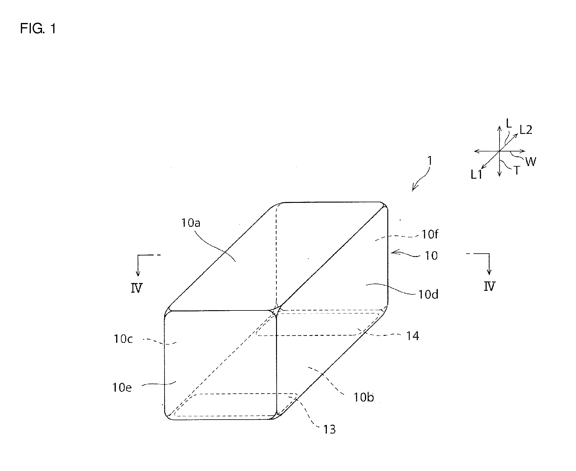
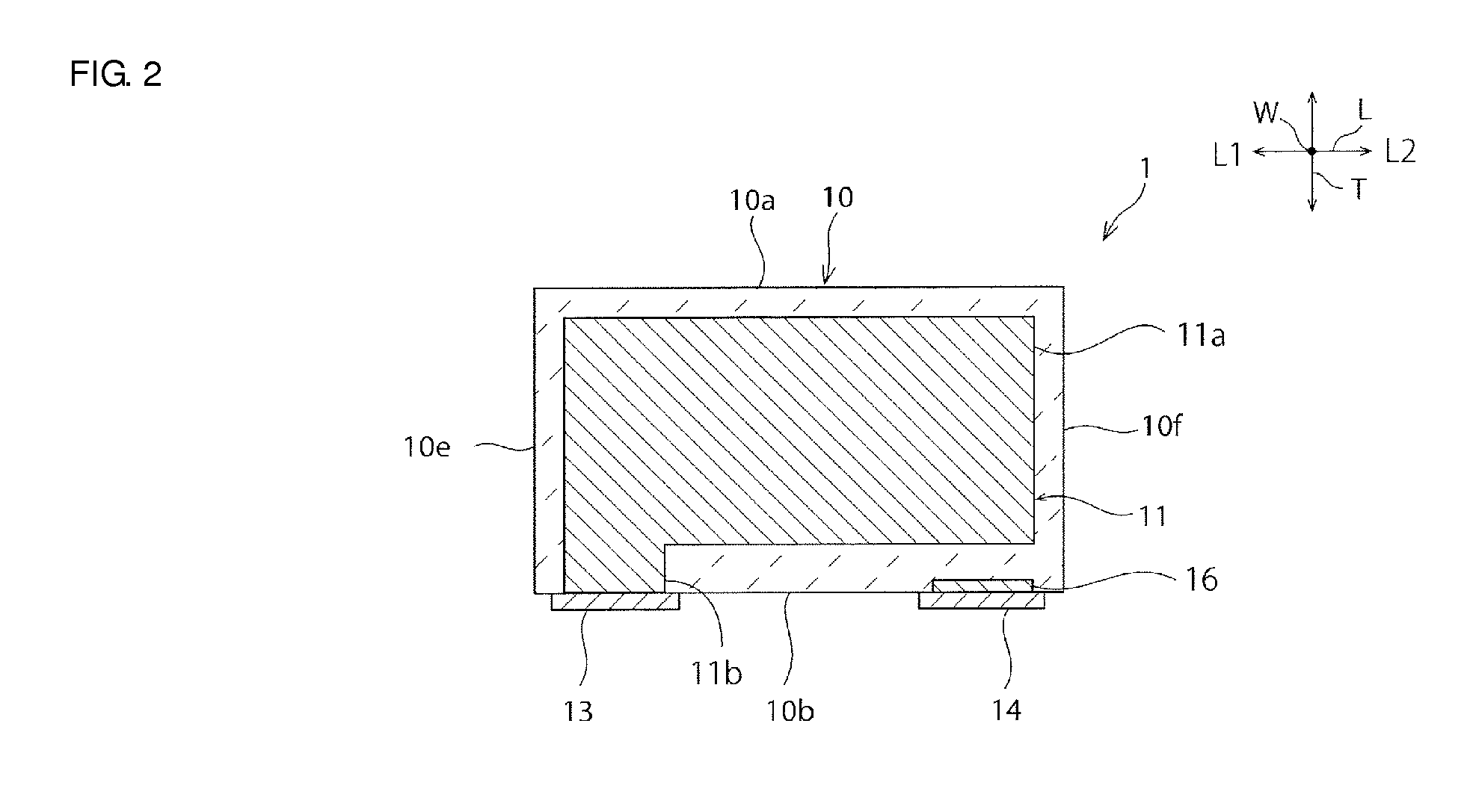
[0066]Eighty ceramic element assemblies having substantially the same configuration as the configuration of the ceramic element assembly 10 of the ceramic electronic component 1 according to the above-described preferred embodiment were produced by the manufacturing method explained in the above-described first preferred embodiment under the following condition.
[0067]Predetermined dimension of ceramic capacitor: length: 3.34 to 3.45 mm, width: 1.82 to 1.85 mm, height: 1.84 to 1.86 mm
[0068]Material for ceramic element assembly: barium titanate based dielectric ceramic
[0069]Primary component of inner electrode: Ni
[0070]Inner electrode pattern: patterns shown in FIG. 5 to FIG. 7
[0071]Predetermined thickness of inner electrode: 0.68 μm
[0072]The total number of inner electrodes: 368 layers
[0073]Predetermined thickness of ceramic layer: 3.6 μm
experimental example 2
[0074]Eighty ceramic element assemblies were produced as with Example 1 except that the mother laminate having the form shown in FIG. 10 was produced.
[0075]The ceramic element assemblies produced in Experimental examples 1 and 2 were immersed into an ink. Thereafter, polishing was performed parallel to the thickness direction T from a second principal surface toward a first principal surface until the lead portions of the first and second inner electrodes were removed so as to expose a cross-section. Whether the ink was impregnated into the facing portions of the plurality of first and second inner electrodes of the cross-section was examined by observation with an optical microscope at a magnification of 200 times or 500 times. A ceramic element assembly in which impregnation with the ink was observed was assumed that peeling between the ceramic green sheets or between the ceramic green sheet and the inner electrode occurred. The results are shown in Table 1 below.
TABLE 1Experiment...
PUM
| Property | Measurement | Unit |
|---|---|---|
| thickness | aaaaa | aaaaa |
| thickness | aaaaa | aaaaa |
| thickness | aaaaa | aaaaa |
Abstract
Description
Claims
Application Information


