Bolometric Detector With A Temperature-Adaptive Biasing

a detector and temperature-adaptive technology, applied in the field of bolometric infrared imaging and pyrometry, can solve the problems of limiting the performance of the detector, affecting the accuracy of the detector, and drowning of useful signals relative to the scene in this background component, so as to improve the signal-to-noise ratio performance and improve the manufacturing cost

Active Publication Date: 2014-08-28
ULIS SAS
View PDF1 Cites 9 Cited by
  • Summary
  • Abstract
  • Description
  • Claims
  • Application Information

AI Technical Summary

Benefits of technology

[0131]Another object of the invention is to provide a detector substantially more tolerant than detectors of the reference technique at the level of the D.C. operation power supplies. This results, on the one hand, in a more extended scene dynamic range-operational temperature range couple and, on the other hand, in an improvement of the signal-to-noise ratio performance with an improved manufacturing cost.

Problems solved by technology

Such a detector has many advantages in terms of manufacturing cost and of use, but also disadvantages which may limit its performance in the absence of specific precautions.
More specifically, a problem of drift of the average signal at the output of the bolometers is posed when the substrate temperature varies afterwards, in particular, changes of external conditions, which are essentially reflected by thermal conduction through the integrated system elements all the way to the substrate level, which defines the average temperature of the sensitive membranes.
As a result, in the absence of specific precautions, the useful signal relative to the scene is drowned in this background component deprived of any interest.
Such means however make the component more complex and expensive and imply an electric power consumption which is all the higher as the ambient temperature is distant from the selected stabilization temperature.
However, the manufacturing cost of such bolometric detectors and the electric power consumption of the system which implements them are precisely the major issue of such detectors.
If, ideally, a perfect rejection is obtained whatever the substrate temperature, in practice, limitations appear when the variations, particularly positive, relative to the reference temperature exceed a few tens of degrees.
Thus, the previously-indicated phenomena limit the operating temperature range of the detector.
Another limitation has to do with the natural dispersion of the values of the bolometric detection and compensation resistances.
Another limitation is due to natural response dispersions, appearing at the denominator in relation (1), usually of technological origin, of active bolometers 16.
Such dispersions also very significantly contribute to limiting the scene dynamic range, all the more as the observed scene is at a high temperature.
As a result, although they are efficient in terms of stability and dispersion of the corrected signal, they do not address the problem of the progressive scene dynamic range loss when the ambient temperature increases.
However, this type of correction requires a constraining calibration and implementation protocol, which requires a complex circuit with digital-to-analog converters associated with memories external to the read circuit, to manage, for each frame, the individualized biasing of each bolometer.
Further, the in-service modification of the biasings offsets in spatially distributed manner, that is non-uniformly, the operation settings of the suspended membranes with respect to factory calibration conditions, and results in a loss of accuracy, which loss is variable according to the ambient conditions, on gain corrections initially calibrated in factory.
This results in an alteration of the image quality.
However, this technique first makes up for the absence of thermalized compensation bolometer directly in the signal forming.
Now, an essential limitation connected to the absence of compensation bolometer in the “offset branch” is the need to decrease the bias voltage of detection bolometers when the substrate temperature increases, substantially by the same proportion as the detection bolometer resistance decrease.
However, the signal-to-noise ratio of a bolometer substantially degrades when the bias voltage decreases.
As a result, the performance of the detector according to this technique more rapidly degrades with temperature than if the biasing was maintained in the vicinity of its nominal and optimal in-factory setting point.
Further, the dynamic principle of the feedback results in eliminating from the useful signal variations due to the average scene temperature.
There is thus no more direct way of knowing this temperature, in other words, such a system is not applicable in thermography.

Method used


Image

  • Bolometric Detector With A Temperature-Adaptive Biasing
  • Bolometric Detector With A Temperature-Adaptive Biasing
  • Bolometric Detector With A Temperature-Adaptive Biasing

Examples


first embodiment

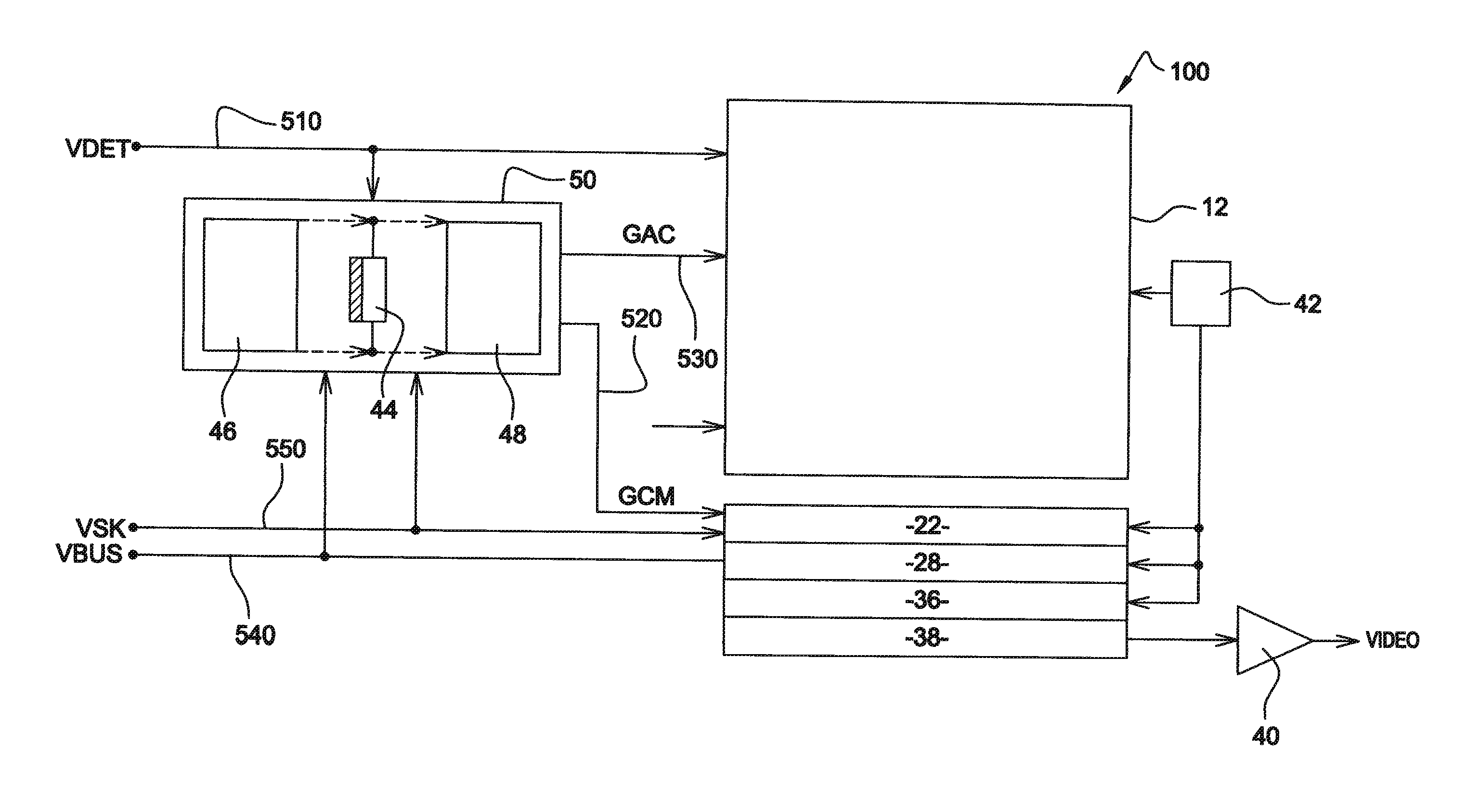
[0149]FIG. 4 illustrates analog circuit 50 for controlling the gate voltages of biasing transistors 18 and 26. Circuit 50 is powered at its input between potentials VSK, carried by a power supply line 550, and VDET, carried by a power supply line 510, and outputs voltages GCM and GAC respectively conveyed by control buses 520 and 530.

[0150]Circuit 50 comprises three parallel current branches 52, 54, and 56 connected between voltage VSK and voltage VDET. Circuit 50 is driven from branch 56, formed of a programmable constant current generator 563 for example, over 3 bits, which injects a constant current I1 into branch 56 through a first MOS transistor 561 and series-connected resistors 512c and 562.

[0151]“Constant current”, means that nominally, there is no need to modify current I1 for the detector to operate according to the invention over the entire envisaged temperature range. It should however be clear that for reasons unconnected to the context of the invention, it may be usefu...

second embodiment

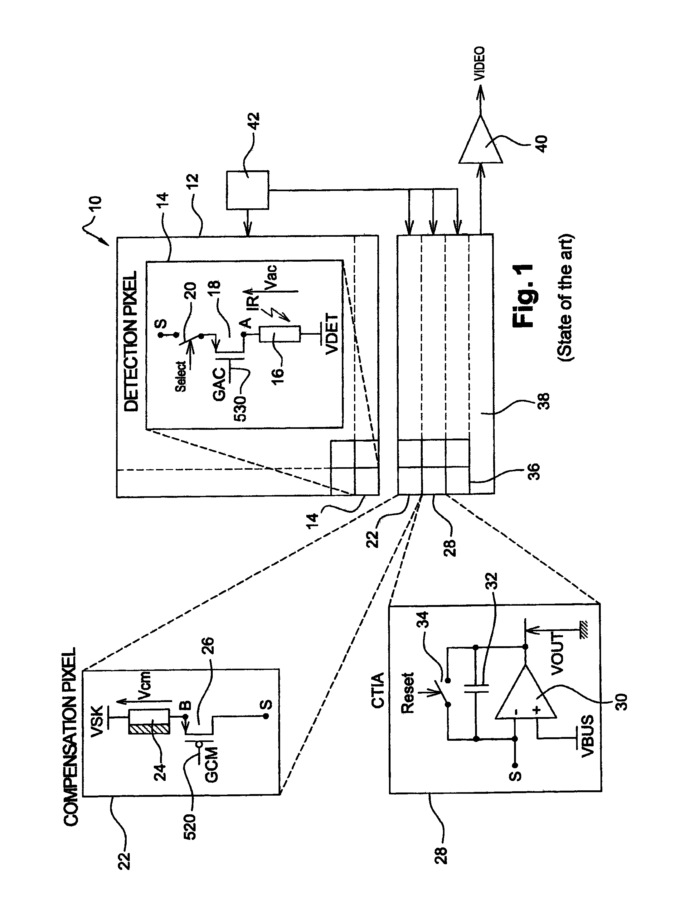
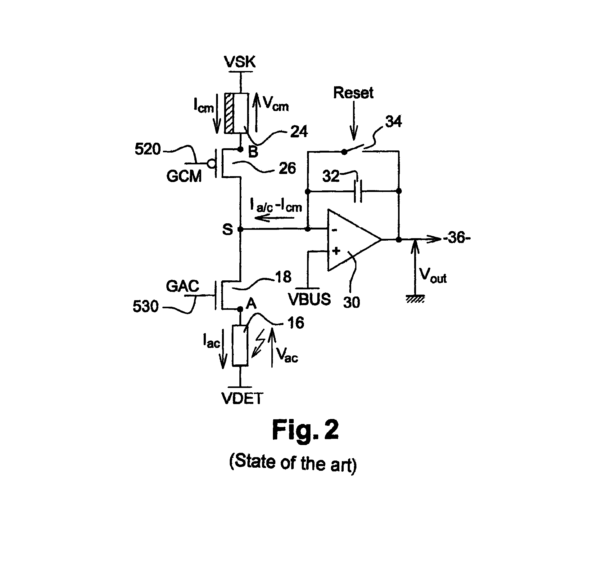
[0204]FIG. 7 is an electric diagram of circuit 50 for controlling the gate voltages of bias transistors 18 and 26 of detection and compensation bolometers 16 and 24.

[0205]The second embodiment comprises, like the first embodiment, current branches 54, 56 and operational amplifiers 531, 532. Unlike the first embodiment, which comprises third current branch 52, in the second embodiment, the outputs of operational amplifier 531, 532 are looped in follower mode onto their inverting inputs to reproduce potentials VB′ and VA′ across MOS transistor 541, and respectively connected to control buses 530, 520.

[0206]Circuit 100 according to the second embodiment comprises two direct-injection buffers 160, 260 connected to buses 530, 520 and to bias transistors 18, 26 of detection bolometer array 12. More specifically, buffers 160, 260 each comprise an operational amplifier having its non-inverting inputs respectively connected to control buses 530, 520. The inverting input and the output of ope...

third embodiment

[0210]According to this third embodiment, circuit 50 is associated with a CTIA integrator 28b totally similar to the CTIA integrators 28 installed at the end of each column of the usual read circuit. Potential VBUS is applied to median point C of circuit 50 via the non-inverting input of the amplifier of integrator 28b. Integrator 28b is reset to zero after each reading of a line of array 12 of detection bolometers 16 by the same control signal Reset as integrators 28b, applied to the controllable switch of integrator 28b. The output of integrator 28b is transmitted to a video amplifier 40b, identical to video amplifier 40, via a sample-and-hold device 36b, identical to sample-and-hold devices 36 and activated in phase therewith. Amplifier 40b, for example of follower amplifier type, outputs a reference signal Video-ref corresponding to the integration of the differential current I522−I521 of half-branches 521, 522 of branch 52 previously described in relation with FIG. 4. More spec...


PUM


Abstract

An infrared detector including an array of detection bolometers each having a bolometric membrane suspended above a substrate, and associated with each bolometer: a detection branch, including the bolometer and a circuit performing a biasing according to a voltage set point, a compensation branch, including a compensation bolometer thermalized to the substrate, a circuit performing a biasing according to a voltage set point, an integrator for generating a voltage by integrating a difference between the currents flowing through said branches, a circuit generating a quantity depending on substrate temperature, including: a bolometer thermalized to the substrate, and a circuit for biasing the bolometer, and a circuit for generating the voltage set points according to said quantity. When the array is exposed to a uniform reference scene, the average of the differences between currents flowing through said branches is within the integrator dynamic range for a substrate temperature range from −30° C.-90° C.

Description

FIELD OF THE INVENTION[0001]The present disclosure relates to the field of bolometric infrared imaging and pyrometry. More specifically, the invention relates to bolometric infrared detectors comprising an array of bolometers formed of membranes suspended above a substrate.BACKGROUND OF THE INVENTION[0002]In the field of so-called “thermal” infrared detectors, it is known to use one-dimensional or two-dimensional arrays of elements sensitive to infrared radiation, capable of operating at ambient temperature.[0003]A thermal infrared detector conventionally uses the variation of a physical quantity of a so-called “thermometric” or “bolometric” material, according to its temperature. Most currently, this physical quantity is the electric resistivity of said material, which is strongly temperature-dependent. The unit sensitive elements of the detector, or “bolometers”, are usually in the form of membranes, each comprising a layer of thermometric material, and suspended above a substrate...

Claims


Application Information

Patent Timeline
Patent Type & Authority Applications(United States)
IPC IPC(8): G01J5/20
CPCG01J5/20G01J5/22H04N5/33H04N25/673
Inventor VILAIN, MICHELROBERT, PATRICK
Owner ULIS SAS
Why Eureka
Try Eureka