Deriving effective corners for complex correlations

a complex correlation and effective corner technology, applied in the field of semiconductor design, can solve the problems of extreme leakage, difficult or nearly impossible control of line-width cd-variation, and considerable challenge in achieving reasonable yield in light of manufacturing variability

Active Publication Date: 2014-09-11
ORACLE INT CORP
View PDF0 Cites 2 Cited by
  • Summary
  • Abstract
  • Description
  • Claims
  • Application Information

AI Technical Summary

Problems solved by technology

In deep submicron processes, the issue of achieving reasonable yield in light of manufacturing variability is a considerable challenge.
In such technologies, for example, channel dopants are in concentrations on the order of fewer than 100 atoms with uncontrollable fluctuations from one device to another; line-width Cd-Variation becomes difficult or nearly impossible to control despite recent advances in lithography techniques; leakage becomes extreme; and electrons exhibit direct tunneling through dielectrics almost as if the dielectrics were not present.
In addition to these limitations of solid state device physics, manufacturing technologists face other difficulties in fabricating circuit structures, such as ultra-deep ultra-violet lithography, optical phase correction (OPC), stepper control, phase shift masks (PSM), chemical mechanical polishing (CMP), depth of field correction (DOF), immersion lithography, etc.
These issues manifest uncertainty, variation, and great difficulty in controlling and managing manufacturing processes, which can result in tremendous yield loss.
This approach can provide reasonable results for smaller circuits and small numbers of varying design metrics, but they may be unable to practically provide meaningful results in context of entire, typically larger and more complex, semiconductor devices having many associated design variables.
These general-purpose process corners are often non-physical and / or unrealistic, and may not explore sensitivities that can be critical to metrics of concern for a given circuit or circuit path.
If not, achieving a reasonable yield can force appreciable trade-offs, which can become so severe as to produce a non-overlapping zero-yielding solution (e.g., when manufacturing engineers try to improve the yield by shifting the process, they can improve a Circuit A at the cost of hindering a Circuit B).
As the process is offset or shifted to accommodate the Level 2 Cache yield, the data path yield may start to decline.
Therefore, satisfying a wafer's parametric yield does not necessarily mean that all the circuits contained on the wafer will likewise have satisfactory yield.

Method used


Image

  • Deriving effective corners for complex correlations
  • Deriving effective corners for complex correlations
  • Deriving effective corners for complex correlations

Examples


Embodiment Construction

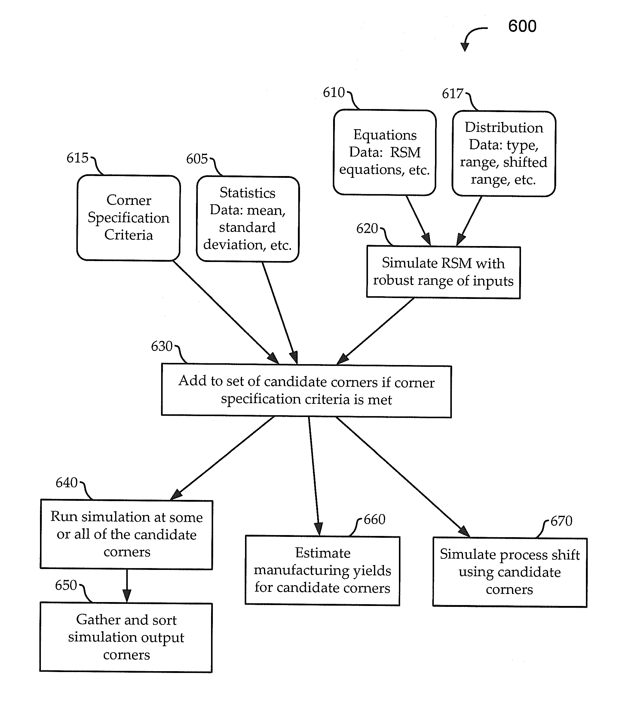
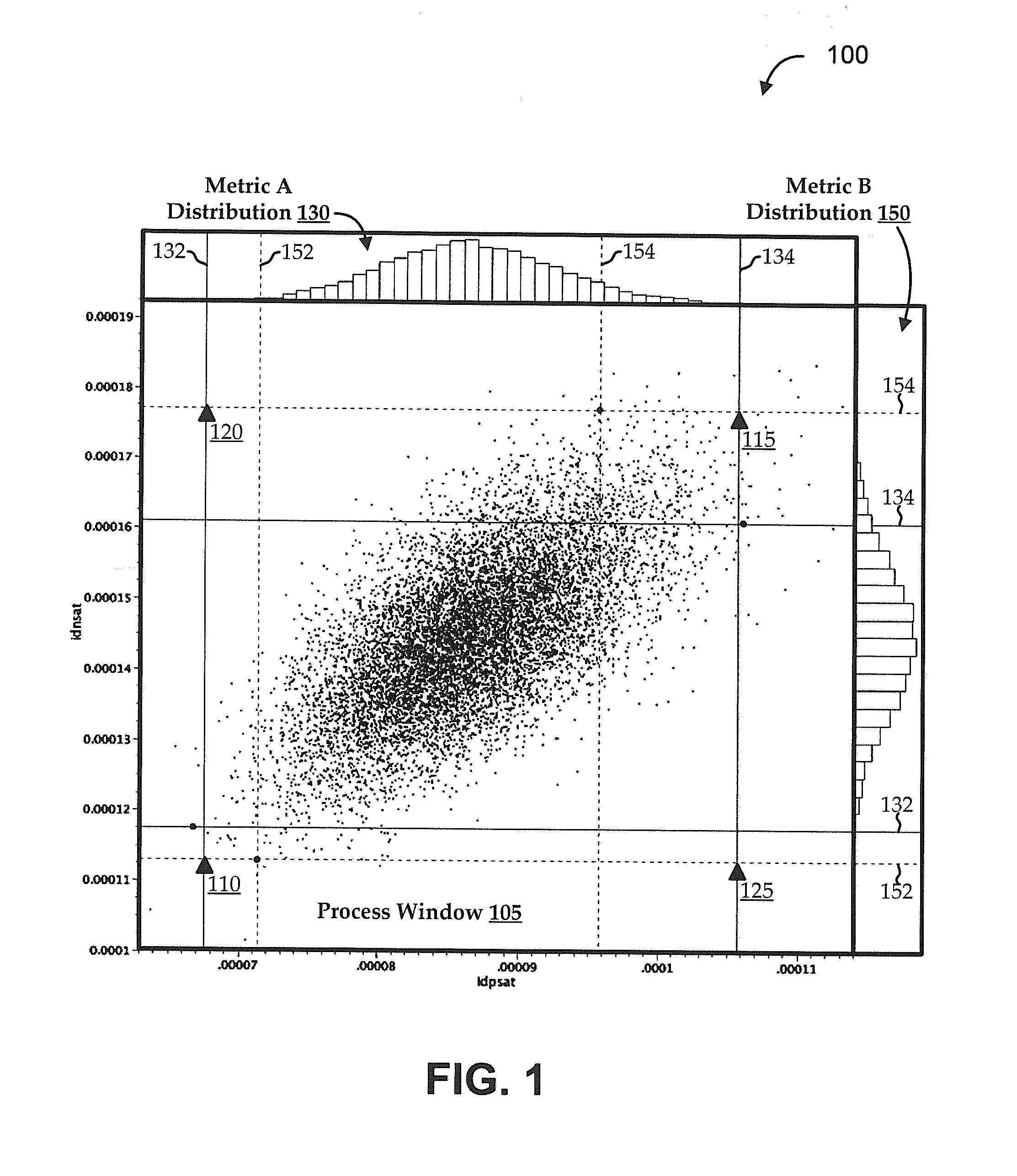
[0016]It has become increasingly common for circuit design efforts to include process design. For example, newer circuit designs often push the limits of available process technologies. Even when existing manufacturing processes are used, the tolerances, complexities, and other features of those processes can impact design of the circuits being manufactured using those processes. Variations in these process parameters, circuit metrics, and / or other factors (generally referred to herein as “metrics”) can each impact yield. Accordingly, achieving a desired effective yield for a full circuit product (e.g., a microprocessor having a number of sub-circuits) can involve modeling, analyzing, and designing in a manner that simultaneously accounts for multiple of those metrics.

[0017]For example, during the design of semiconductor devices (e.g., single transistors, circuits, chips, wafers, etc.), circuit simulations, like post-layout circuit simulations, may be performed using a net-list extr...


PUM


Abstract

Systems and methods are described for simultaneously deriving an effective x-sigma corner for multiple, different circuit and / or process metrics for a semiconductor device. The result is an effective sigma that is representative of design intent. Some implementations account for covariance, and use joint probability as the criteria for the effective x-sigma corner (e.g., as opposed to a unique sigma level of each individual metric). Analysis results for each metric can be transformed to metric distributions in a common distribution framework, and a correlation matrix can be calculated. The transformed metric distributions can be input to a joint probability distribution set to achieve a target joint sigma level. The joint probability distribution and correlation matrix values can be used to back-calculate scaled x-sigma corners for each metric distribution. Simulation of the device can be performed at one or more of the scaled x-sigma corners.

Description

FIELD[0001]Embodiments relate generally to semiconductor design, and, more particularly, to multi-dimensional yield analysis for manufacturing of semiconductor designs.BACKGROUND[0002]In deep submicron processes, the issue of achieving reasonable yield in light of manufacturing variability is a considerable challenge. At approximately the 130 nm process node, the underlying physics and quantum mechanical effects begin to govern the behavior of CMOS technology and the ability to dictate and predict the desired behavior begins to decline. In such technologies, for example, channel dopants are in concentrations on the order of fewer than 100 atoms with uncontrollable fluctuations from one device to another; line-width Cd-Variation becomes difficult or nearly impossible to control despite recent advances in lithography techniques; leakage becomes extreme; and electrons exhibit direct tunneling through dielectrics almost as if the dielectrics were not present. In addition to these limita...

Claims


Application Information

Patent Timeline
Patent Type & Authority Applications(United States)
IPC IPC(8): G06F17/50
CPCG06F17/5081G06F30/398G06F2111/08
Inventor BARKER, AARON J.
Owner ORACLE INT CORP
Why Eureka
Try Eureka